Final Degree Thesis corazón, ¡muchas gracias a todos! Raúl Macías Macías vi TABLE OF CONTENTS...
74
Final Degree Thesis Towards Wearable Spectroscopy Bioimpedance Applications Power Management for a Battery Driven Impedance Meter By RAÚL MACÍAS MACÍAS FINAL DEGREE THESIS 30 ECTS, ERASMUS, SWEDEN ELECTRICAL ENGINEERING SPECIALIZATION IN COMMUNICATIONS & SIGNAL PROCESSING THESIS Nº 5/2009
Transcript of Final Degree Thesis corazón, ¡muchas gracias a todos! Raúl Macías Macías vi TABLE OF CONTENTS...
Final Degree Thesis Towards Wearable Spectroscopy
Bioimpedance Applications Power Management for a Battery Driven Impedance Meter
By
RAÚL MACÍAS MACÍAS
FINAL DEGREE THESIS 30 ECTS, ERASMUS, SWEDEN ELECTRICAL ENGINEERING SPECIALIZATION IN COMMUNICATIONS & SIGNAL PROCESSING
THESIS Nº 5/2009
Towards Wearable Spectroscopy Bioimpedance Applications: Power
Management for a Battery Driven Impedance Meter
Raúl Macías Macías
Master Thesis
Subject Category: Technology. Biomedical Signal Processing
Series Number Communication and Signal Processing
University of Borås
School of Engineering
SE- 501 90 BORÅS
Telephone +46 33 435 4640
Examiner: Fernando Seoane Martínez
Supervisor: Fernando Seoane Martínez
Date: 2009 May 19th
Keyword: Electrical Bioimpedance, Wearable Medical Device, Power Management,
Labview, Smart Textiles.
iii
ABSTRACT
In recent years, due to the combination of technological advances in the fields of measurement instrumentation, communications, home-health care and textile-technology the development of medical devices has shifted towards applications of personal healthcare.
There are well known the available solutions for heart rate monitoring successfully provided
by Polar and Numetrex. Furthermore new monitoring applications are also investigated. Among these non-invasive monitoring applications, it is possible to find several ones enable by measurements of Electrical Bioimpedance.
Analog Devices has developed the AD5933 Impedance Network Analyzer which facilitates
to a large extent the design and implementation of Electrical Bioimpedance Spectrometers in a much reduced space. Such small size allows the development of a fully wearable bioimpedance measurement.
With the development of a Electrical Bioimpedance-enable wearable medical device in focus
for personal healthcare monitoring, in this project, the issue of power management has been targeted and a battery-driven Electrical Bioimpedance Spectrometer based in the AD5933 has been implemented. The resulting system has the possibility to operate with a Li-Po battery with a power autonomy over 17 hours.

v
ACKNOWLEDGEMENTS
En primer lugar me gustaría dedicar este trabajo a mis padres, Nino y Antonia, y a mis
abuelos, Franciso e Isabel y Demetrio e Isabel, por el cariño y amor brindados en todos estos años. Gracias también por haberme cuidado, apoyado y educado como lo habéis hecho así como por haber confiado en mí y haberme dejado la libertad de decidir por mí mismo en todo momento.
También me gustaría agradecer a todos mis amigos todos los momentos compartidos, tanto
los buenos como los no tan buenos, y el apoyo recibido. Gracias a todos por haberme hecho disfrutar todos estos años y por haberme animado cuando era necesario.
Gracias también a todos los compañeros que he conocido en mi experiencia Erasmus por
haberme ayudado a sentirme como en casa y brindarme su amistad desde el primer momento. También agradecer a Ramon Bragós, y a todo los compañeros del Laboratorio de
Instrumentación y Bioingeniería de la UPC, la paciencia y la gran ayuda ofrecida. Por último, agradecer a mi supervisor, Dr. Fernando Seoane, toda la paciencia que ha tenido
conmigo. Gracias por haberme ayudado a conocer un poco más el mundo de la bioingeniería y por haberme facilitado tanto las cosas en mi experiencia Erasmus, tanto a nivel de estudios como a nivel personal.
De corazón, ¡muchas gracias a todos! Raúl Macías Macías
vi
TABLE OF CONTENTS
CHAPTER 1 INTRODUCTION ................................................................................................................. 3
1.1. INTRODUCTION ................................................................................................................................ 3
1.2. MOTIVATION ..................................................................................................................................... 3
1.3. GOAL .................................................................................................................................................... 3
1.4. WORK DONE ...................................................................................................................................... 3
1.5. STRUCTURE OF THE THESIS REPORT ...................................................................................... 4
1.6. OUT OF SCOPE .................................................................................................................................. 4
CHAPTER 2 BACKGROUND ................................................................................................................... 5
2.1. BIOIMPEDANCE (EBI) ..................................................................................................................... 5
2.1.1. ELECTRICAL PROPERTIES OF TISSUE [1] ............................................................................................. 5 2.1.2. TISSUE AS DISPERSIVE MEDIUM [1] ................................................................................................... 7
2.1.2.1. α-dispersion .................................................................................................................................... 7 2.1.2.2. β-dispersion .................................................................................................................................... 7 2.1.2.3. γ-dispersion ..................................................................................................................................... 8 2.1.2.4. δ-dispersion .................................................................................................................................... 8
2.1.3. ELECTRICAL MODEL OF CELLS .......................................................................................................... 8
2.2. BODY COMPOSITION & BIOIMPEDANCE ANALYSIS (BIA) ............................................... 11
2.2.1. BODY COMPOSITION COMPARTMENTS [6] ........................................................................................ 11 2.2.1.1. Fat Free Mass (FFM) ................................................................................................................... 11 2.2.1.2. Total Body Water (TBW) .............................................................................................................. 11 2.2.1.3. Intracellular Water (ICW) ............................................................................................................ 12 2.2.1.4. Extracellular Water (ECW) .......................................................................................................... 12 2.2.1.5. Fat Mass (FM) .............................................................................................................................. 12
2.2.2. INTRODUCTION TO BIA [6] ............................................................................................................... 12 2.2.3. METHODS OF BIA [6] ....................................................................................................................... 13
2.2.3.1. Single Frequency BIA (SF-BIA) ................................................................................................... 13 2.2.3.2. Multi-Frequency BIA (MF-BIA) ................................................................................................... 14 2.2.3.3. Bioelectrical Spectroscopy (BIS) .................................................................................................. 14 2.2.3.4. Segmental-BIA .............................................................................................................................. 15 2.2.3.5. Localized BIA ............................................................................................................................... 16 2.2.3.6. Bioelectrical Impedance Vector Analysis (BIVA) [12] ................................................................. 16
2.3. ELECTRODES & EBI MEASUREMENT [1] ................................................................................ 17
2.3.1. INTRODUCTION TO SKIN-ELECTRODE INTERFACE ............................................................................ 17 2.3.2. EBI MEASUREMENT CONFIGURATIONS ............................................................................................ 18
2.3.2.1. Two-Electrode Measurement ........................................................................................................ 18 2.3.2.2. Four-Electrode Measurement ....................................................................................................... 19
2.4. WEARABLE MEDICAL DEVICES [13] ........................................................................................ 20
2.4.1. INTRODUCTION TO WEARABLE MEDICAL DEVICES .......................................................................... 20 2.4.2. DESIGN REQUIREMENTS & CHALLENGES OF WMDS ....................................................................... 20
CHAPTER 3 SYSTEM DESIGN AND ITS IMPLEMENTATION ...................................................... 21
3.1. SYSTEM DESIGN HARDWARE .................................................................................................... 21
vii
3.1.1. INTRODUCTION ................................................................................................................................. 21 3.1.2. POWER MANAGEMENT BLOCK ......................................................................................................... 21
3.1.2.1. Introduction .................................................................................................................................. 21 3.1.2.2. MAX8677 ...................................................................................................................................... 22 3.1.2.3. MAX1763 ...................................................................................................................................... 26
3.1.3. EBI BLOCK ...................................................................................................................................... 29 3.1.3.1. Introduction .................................................................................................................................. 29 3.1.3.2. AD5933 ......................................................................................................................................... 29
3.1.4. IMPLEMENTATION BOARD ................................................................................................................ 32
3.2. SOFTWARE IMPLEMENTATION ................................................................................................ 33
3.2.1. INTRODUCTION ................................................................................................................................. 33 3.2.2. I2C PROTOCOL [15] [16] [17] ........................................................................................................... 34
3.2.2.1. I2C Introduction ........................................................................................................................... 34 3.2.2.2. I2C Bus Characteristics ................................................................................................................ 34 3.2.2.3. I2C Protocol ................................................................................................................................. 35
3.2.3. LABVIEW APPLICATION .................................................................................................................... 36 3.2.3.1. Introduction .................................................................................................................................. 36 3.2.3.2. AD5933 Configuration Blocks ...................................................................................................... 36 3.2.3.3. Impedance Magnitude Calculation ............................................................................................... 39 3.2.3.4. Impedance Phase Calculation ...................................................................................................... 41
CHAPTER 4 MEASUREMENTS AND VALIDATION ........................................................................ 42
4.1. BOARD ELECTRICAL CHARACTERISTICS ............................................................................. 42
4.1.1. BATTERY LIFE .................................................................................................................................. 42
4.2. EBI MEASUREMENTS .................................................................................................................... 43
4.2.1. RESISTANCE MEASUREMENTS .......................................................................................................... 43 4.2.2. RC CIRCUIT TOPOLOGY MEASUREMENTS ........................................................................................ 47 4.2.3. BIOLOGICAL MEASUREMENTS .......................................................................................................... 50
4.3. MEASUREMENT VALIDATION ................................................................................................... 51
4.3.1. NOISE INFLUENCE IN MEASUREMENTS ............................................................................................. 51 4.3.2. TEMPERATURE INFLUENCE IN MEASUREMENTS ............................................................................... 53
CHAPTER 5 CONCLUSIONS & FUTURE WORK .............................................................................. 55
5.1 GENERAL CONCLUSIONS ..................................................................................................................... 55
5.2. FUTURE WORK ....................................................................................................................................... 56
5.2.1. FRONT-END ...................................................................................................................................... 56 5.2.2. EMBEDDED SYSTEM ......................................................................................................................... 56
REFERENCES .................................................................................................................................................. 57
APPENDIX A ORCAD SCHEMATICS .................................................................................................... 59
APPENDIX B LAYOUT ............................................................................................................................. 61
APPENDIX C LABVIEW BLOCKS .......................................................................................................... 63

1
LIST OF ACRONYMS
AC - Alternating Current ADC - Analog-to-Digital Converter AFE - Analog Front-End BCM - Body Cell Mass BIA - Bioelectrical Impedance Analysis BIS - Bioelectrical Impedance Spectroscopy BIVA - Bioelectrical Impedance Vector Analysis DAC - Digital-to-Analog Converter DC - Direct Current DDS - Direct Digital Synthesizer DFT - Discrete Fourier Transform DSP - Digital Signal Processor EBI - Electrical Bio Impedance ECF - Exta-Cellular Fluid ECW - Extra-Cellular Water EMB - Electrical-bioimpedance Measurement Block I2C - Inter-Integrated Circuit IC - Integrated Circuit ICW - Intra-Cellular Water IP - International Protection I/O - Input/Output FFM - Fat-Free Mass FM - Fat Mass LiPo - Lithium-ion Polymer LSB - Least Significant Bit MF-BIA - Multi- Frequency Bioelectrical Impedance Analysis MSB - Most Significant Bit NI - National Instruments OVP - Over-Voltage Protection PC - Personal Computer PGA - Programmable Gain Amplifier PMB - Power Management Block PWM - Pulse-Width Modulation SF-BIA - Single- Frequency Bioelectrical Impedance Analysis SMBus - System Management Bus SMD - Surface Mount Device SPI - Serial Peripheral Interface TBW - Total Body Water TUS - Tissue Under Study USB - Universal Serial Bus WMD - Wearable Medical Device

3
CHAPTER 1
INTRODUCTION
1.1. Introduction New methods and devices are constantly required in medicine. Nowadays, there are two
important branches of investigation. On the one hand, new methods as minimally invasive as possible for patients are developed. In this sense, Electrical Bioimpedance (EBI) method has been proved as a good solution. As EBI measurements detect changes in the structure and composition of tissues produced by pathophysiological processes, they are used as tool for the diagnosis of some diseases as well as tool for assessing body composition.
On the other hand, new devices are required to monitor continuously some body parameters. These devices should be as wearable as possible to make patient’s life easier.
1.2. Motivation In recent years, the concern for designing medical devices as comfortable and easy-use as
possible has grown. Furthermore, the Electrical Bioimpedance Measurements have been proved to be suitable for assessing body composition and also for monitoring some physiological parameters.
Due to these two facts, an Electrical Bioimpedance device, as wearable as possible, is proposed in this thesis to monitoring some body parameters minimizing complications in patients’ life.
1.3. Goal The main goal of this thesis is to design and to implement two modules which will be part of
a future wearable medical device. These two modules are the power management block and the impedance converter block. The first one chooses the power source and charges the battery when this is not completely full. The second module target is to measure the load impedance which exists between the input and output pins of the IC manufactured by Analog Devices called AD5933.
Due to this IC uses the I2C communication protocol, a secondary aim is to develop a Labview program to communicate the system with a Master Device and to configure the impedance converter.
1.4. Work done As previously mentioned, the main aim of this project has been the design and the
development of a wearable medical device based on EBI measurements. To reach this, the following tasks have been done:
· Both modules, which are part of the system, were designed by the software called OrCAD. They were designed using Surface Mount Devices (SMDs) to make the design as small and light as possible.
4
· The designed board was implemented by an external company. Later, all SMDs were soldered by hand on the board. · After checking the board worked, a program was implemented in a PC by the software called Labview to configure the on-board IC called AD5933 using the I2C protocol. · Finally, when everything worked, some measurements were acquired to check some board features such as battery life or work range.
1.5. Structure of the Thesis Report The thesis report is organized in five chapters, appendices and references. Chapter 1 is the
introduction part of the thesis. Chapter 2 gives a brief background of Electrical Bioimpedance (EBI) and its application in Measurements of Body Composition, also known as Bioelectrical Impedance Analysis (BIA). Furthermore, Chapter 2 gives a brief idea about using EBI in wearable devices. Chapter 3 explains the on-board designed system using OrCAD. Also, in this chapter the Labview developed software for I2C communication is described. Chapter 4 shows some measurement results; it includes some electrical features of the board and measurements validation. Finally, Chapter 4 is followed by the conclusions and proposed future work in the last chapter.
1.6. Out of Scope The following points have been decided to leave out of this thesis work: ∗ The implementation of an Analog Front-End to enable 4-electrod method for biomedical
applications has been left out because there was other project to this one. ∗ To implement an embedded system is out of scope because there is a future proposal
where the Analog Front-End module, a Bluetooth module and our two modules, the Power Management module and the Impedance Converter module, should be joined and controlled by a microchip.
5
CHAPTER 2
BACKGROUND
In biomedical engineering, EBI is a term used to describe the response of a living organism to an externally applied electric current. It is a measure of the opposition to the flow of electric current through the tissues.
The measurement of EBI of humans and animals has proved useful as a diagnosis and monitoring tool for several applications such as respiration rate, impedance cardiography or body composition, known as bioelectrical impedance analysis or simply BIA.(Seoane, 2007)
2.1. Bioimpedance (EBI)
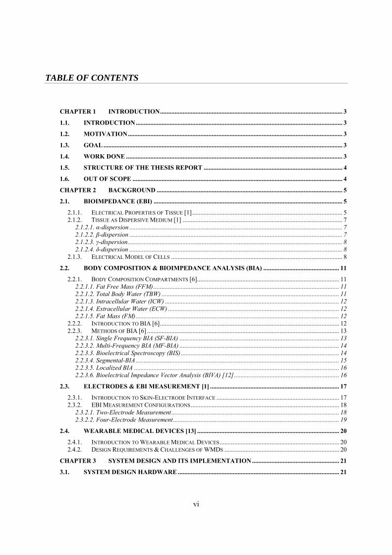
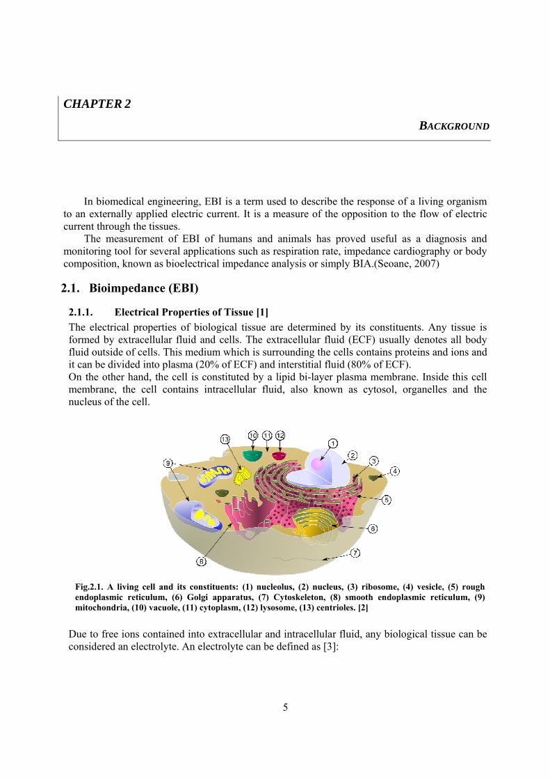
2.1.1. Electrical Properties of Tissue [1] The electrical properties of biological tissue are determined by its constituents. Any tissue is formed by extracellular fluid and cells. The extracellular fluid (ECF) usually denotes all body fluid outside of cells. This medium which is surrounding the cells contains proteins and ions and it can be divided into plasma (20% of ECF) and interstitial fluid (80% of ECF). On the other hand, the cell is constituted by a lipid bi-layer plasma membrane. Inside this cell membrane, the cell contains intracellular fluid, also known as cytosol, organelles and the nucleus of the cell.
Due to free ions contained into extracellular and intracellular fluid, any biological tissue can be considered an electrolyte. An electrolyte can be defined as [3]:
Fig.2.1. A living cell and its constituents: (1) nucleolus, (2) nucleus, (3) ribosome, (4) vesicle, (5) rough endoplasmic reticulum, (6) Golgi apparatus, (7) Cytoskeleton, (8) smooth endoplasmic reticulum, (9) mitochondria, (10) vacuole, (11) cytoplasm, (12) lysosome, (13) centrioles. [2]
6
“Any substance that will dissociate into ions in solution and acquire the capacity to conduct electric current in the presence of an external electrical field.”
Thus biological tissue is also considered an ionic conductor where K+, Na+ and Ca2+ are the most important ions contributing to the ionic current.
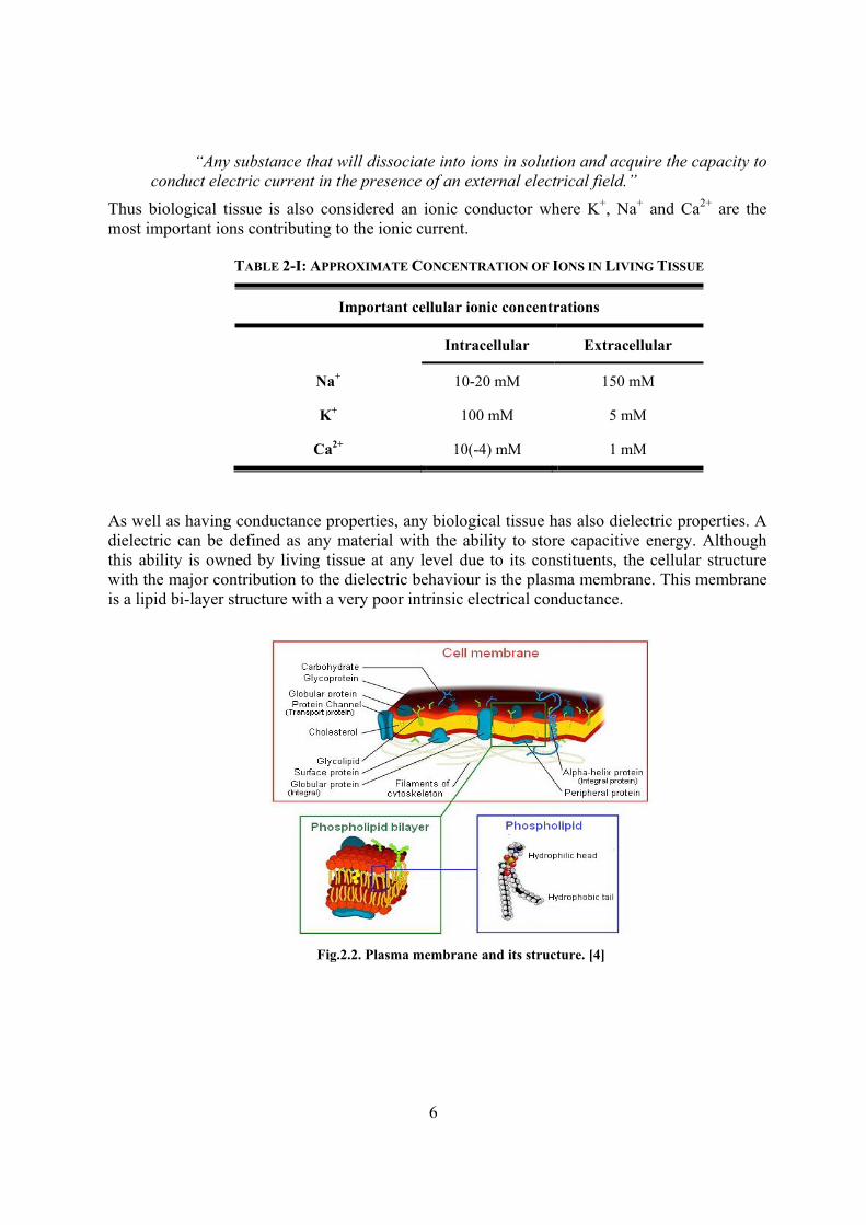
As well as having conductance properties, any biological tissue has also dielectric properties. A dielectric can be defined as any material with the ability to store capacitive energy. Although this ability is owned by living tissue at any level due to its constituents, the cellular structure with the major contribution to the dielectric behaviour is the plasma membrane. This membrane is a lipid bi-layer structure with a very poor intrinsic electrical conductance.
TABLE 2-I: APPROXIMATE CONCENTRATION OF IONS IN LIVING TISSUE
Important cellular ionic concentrations
Intracellular Extracellular
Na+ 10-20 mM 150 mM
K+ 100 mM 5 mM
Ca2+ 10(-4) mM 1 mM
Fig.2.2. Plasma membrane and its structure. [4]
7
Therefore, the structure formed by the intracellular fluid, plasma membrane and extracellular fluid (conductor-dielectric-conductor) behaves as a capacitor with a specific capacitance of 1 µF/cm2.
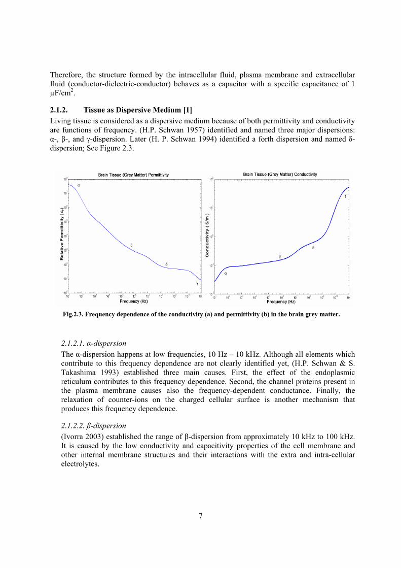
2.1.2. Tissue as Dispersive Medium [1] Living tissue is considered as a dispersive medium because of both permittivity and conductivity are functions of frequency. (H.P. Schwan 1957) identified and named three major dispersions: α-, β-, and γ-dispersion. Later (H. P. Schwan 1994) identified a forth dispersion and named δ-dispersion; See Figure 2.3.
2.1.2.1. α-dispersion The α-dispersion happens at low frequencies, 10 Hz – 10 kHz. Although all elements which contribute to this frequency dependence are not clearly identified yet, (H.P. Schwan & S. Takashima 1993) established three main causes. First, the effect of the endoplasmic reticulum contributes to this frequency dependence. Second, the channel proteins present in the plasma membrane causes also the frequency-dependent conductance. Finally, the relaxation of counter-ions on the charged cellular surface is another mechanism that produces this frequency dependence.
2.1.2.2. β-dispersion (Ivorra 2003) established the range of β-dispersion from approximately 10 kHz to 100 kHz. It is caused by the low conductivity and capacitivity properties of the cell membrane and other internal membrane structures and their interactions with the extra and intra-cellular electrolytes.
Fig.2.3. Frequency dependence of the conductivity (a) and permittivity (b) in the brain grey matter.

8
2.1.2.3. γ-dispersion This dispersion is due to the high content of water in cell and tissue. Its relaxation frequency is nearly about 20 GHz, like normal water, and its range of dispersion is from hundreds of MHz to some GHz.
2.1.2.4. δ-dispersion This dispersion is a weak relaxation between β-, and γ-dispersion. It occurs from around 300 MHz to around 2 GHz. This dispersion is caused by rotation of amino acids, partial rotation of charge side groups of proteins, and proteins bonded to water.
The main and more interesting dispersions in medical applications are α- and β-dispersions. In these range is where most changes between pathological and normal tissue occur (Blad B. 1996 Nov). Finally, in the Table 2-II the four dispersion windows and the elements that contribute to each one are shown.
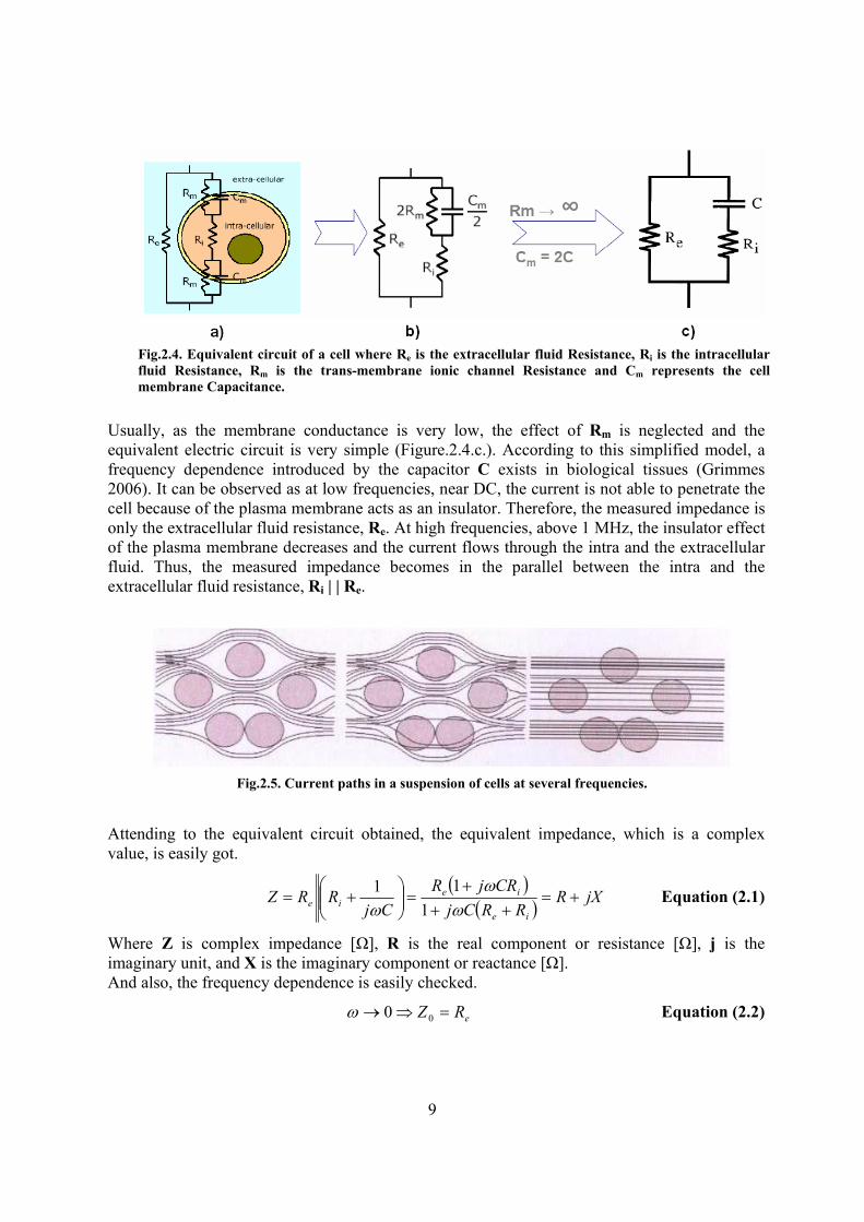
2.1.3. Electrical Model of Cells As previously mentioned, electrical properties of tissue are caused by its constituents. Therefore considering these constituents and applying theory of electrical circuits, an explanatory and descriptive electrical model for the cell can be deduced (Fricke 1924); see Figure 2.4
TABLE 2-II: ELECTRICAL DISPERSIONS OF BIOLOGICAL MATTER*.
Contributing Biomaterial Element
Dispersion α β γ δ
Water and Electrolytes
Biological Macromolecules
Amino acids Proteins Nucleic acids
Vesicles Surface Charged Non-Surface Charged
Cells with Membrane
+ Fluids free of protein + Tubular system + Surface charge + Membrane relaxation + Organelles + Protein
*Table contents from (H. P. Schwan 1994)
9
Usually, as the membrane conductance is very low, the effect of Rm is neglected and the equivalent electric circuit is very simple (Figure.2.4.c.). According to this simplified model, a frequency dependence introduced by the capacitor C exists in biological tissues (Grimmes 2006). It can be observed as at low frequencies, near DC, the current is not able to penetrate the cell because of the plasma membrane acts as an insulator. Therefore, the measured impedance is only the extracellular fluid resistance, Re. At high frequencies, above 1 MHz, the insulator effect of the plasma membrane decreases and the current flows through the intra and the extracellular fluid. Thus, the measured impedance becomes in the parallel between the intra and the extracellular fluid resistance, Ri | | Re.
Attending to the equivalent circuit obtained, the equivalent impedance, which is a complex value, is easily got.
( )( ) jXR
RRCjCRjR
CjRRZ
ie
ieie +=
+++
=⎟⎟⎠
⎞⎜⎜⎝
⎛+=
ωω
ω 111 Equation (2.1)
Where Z is complex impedance [Ω], R is the real component or resistance [Ω], j is the imaginary unit, and X is the imaginary component or reactance [Ω]. And also, the frequency dependence is easily checked.
eRZ =⇒→ 00ω Equation (2.2)
Fig.2.4. Equivalent circuit of a cell where Re is the extracellular fluid Resistance, Ri is the intracellular fluid Resistance, Rm is the trans-membrane ionic channel Resistance and Cm represents the cell membrane Capacitance.
Fig.2.5. Current paths in a suspension of cells at several frequencies.
10
ie
ieie RR
RRRRZ+
==⇒∞→ ∞ω Equation (2.3)
The validity of Fricke model for tissues and blood was checked by (Kanai 1983), but it was just correct for blood because it contains one dominant cell species (Jaffrin 1997). As human tissue contains different types of cells, the Cole impedance model was proposed by (K. S. Cole 1940) as a more realistic model for tissue. This model consists of three parts: an equation, an equivalent circuit, and a complex impedance circular arc. [5] The Cole empirical equation for the frequency dependence of tissue or cell suspension complex impedance is
( )αωτjRR
RZ+
−+= ∞
∞ 10 Equation (2.4)
Where Z is complex impedance [Ω], R∞ is the resistance [Ω] at very high frequencies, j is the imaginary unit, R0 is the resistance [Ω] at very low frequencies, ω is the angular frequency [1/s], τ is the characteristic relaxation time constant of the system [s], and α is an exponent [dimensionless] with value 1 as a typical value (single-dispersion). And its equivalent electrical model is based upon the replacement of the ideal capacitor in the Debye model, shown in the Fig.2.6, with a more general constant phase element (CPE).
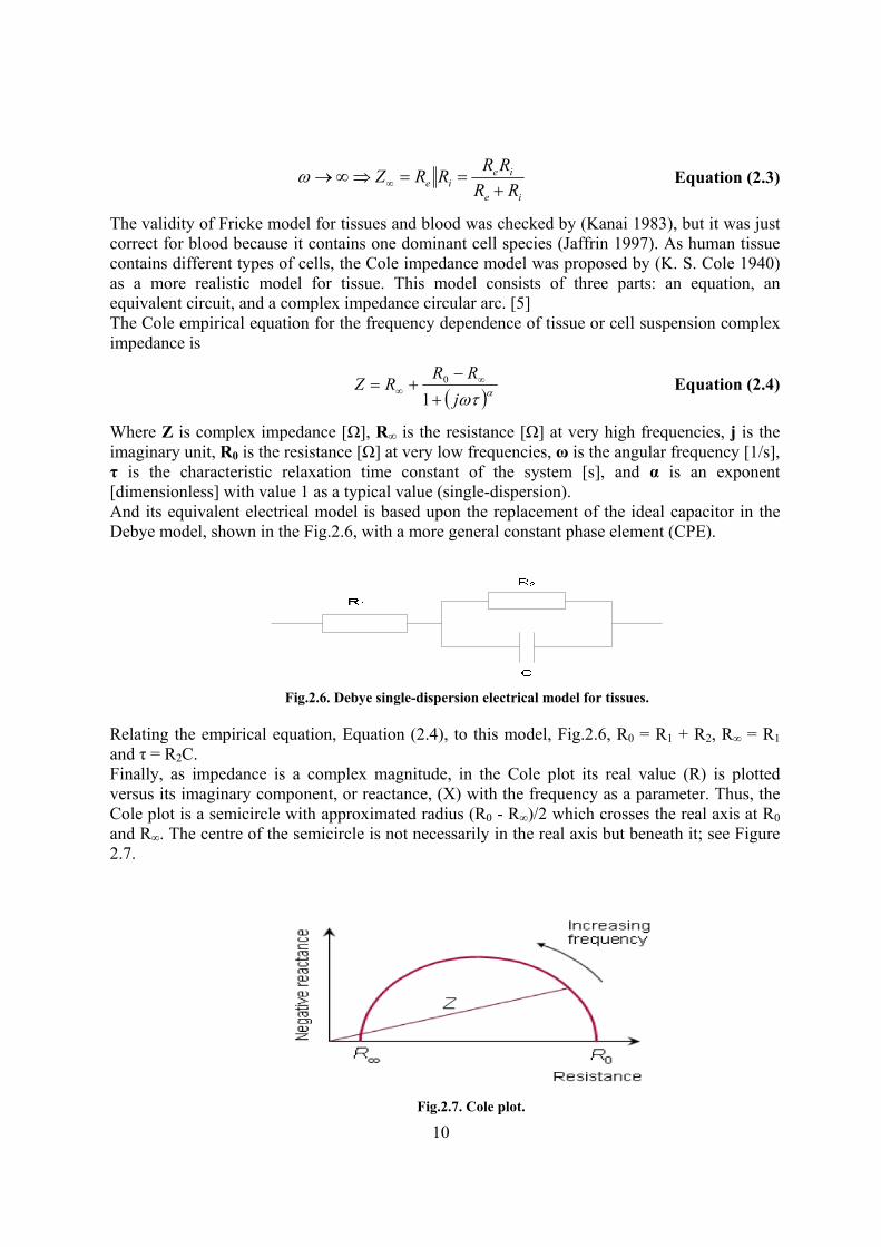
Relating the empirical equation, Equation (2.4), to this model, Fig.2.6, R0 = R1 + R2, R∞ = R1 and τ = R2C. Finally, as impedance is a complex magnitude, in the Cole plot its real value (R) is plotted versus its imaginary component, or reactance, (X) with the frequency as a parameter. Thus, the Cole plot is a semicircle with approximated radius (R0 - R∞)/2 which crosses the real axis at R0 and R∞. The centre of the semicircle is not necessarily in the real axis but beneath it; see Figure 2.7.
Fig.2.6. Debye single-dispersion electrical model for tissues.
Fig.2.7. Cole plot.

11
2.2. Body Composition & Bioimpedance Analysis (BIA)
2.2.1. Body Composition Compartments [6]
Fig.2.8 shows the body composition of a hypothetical, normal weight adult. It can be seen that the major component of the human body is water. The protein and fat component are relatively small, with the remainder being primarily bone and minerals. All these components are usually grouped into different compartments; see Fig.2.9.
2.2.1.1. Fat Free Mass (FFM) The non-fat component of body composition is termed fat free mass, or also lean body mass, and exists primarily as the chief structural and functional component of the human body. This compartment consists in proportions of water (72%), protein (21%) and bone minerals (7%).
2.2.1.2. Total Body Water (TBW) All of the water content of the human body is termed total body water and it can be divided into intra (ICW) and extracellular water (ECW). TBW usually represents around 60% of the body weight but this can vary between 45 and 75% due to primarily to differences in body fat. It is a measure for evaluating basic hydration status.
Fig.2.8. Body Composition of a normal weight Fig.2.9. Schematic diagram of fat-free mass (FFM), male. [7] total body water (TBW), intracellular water (ICW), extracellular water (ECW) and body cell mass (BCM).
12
2.2.1.3. Intracellular Water (ICW) All of the water content inside the cells is termed intracellular water and it represents around 2/3 of the TBW.
2.2.1.4. Extracellular Water (ECW) All of the water outside the cells is termed extracellular water and it represents around 1/3 of TBW.
2.2.1.5. Fat Mass (FM) Fat mass (FM) is all the extractable lipids from adipose and other tissue in the body. It is the total amount of stored lipids, or fats, in the body and consists of subcutaneous fat and visceral fat. Subcutaneous fat is located directly beneath the skin and serves as an energy reserve and as insulation against outside cold. Visceral fat is located deeper within the body and serves as an energy reserve and as a cushion between organs [8]. It is usually determined as Weight minus FFM.
Due to adipose tissue only contains around 10-15% of water and lean, or muscle, contains around 75% of it, an obese person will have less TBW than a sportsman; see Table 2-III.
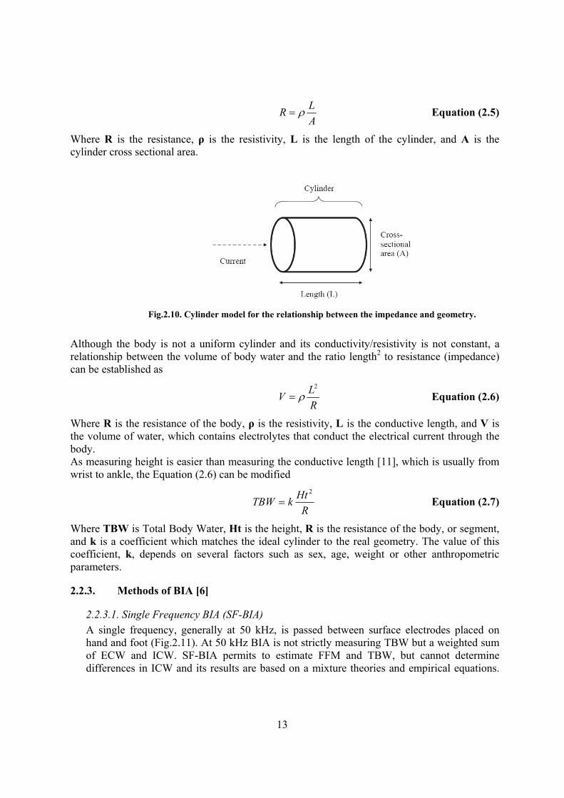
2.2.2. Introduction to BIA [6] Bioelectrical impedance analysis (BIA) is a method which measures the impedance or opposition to the flow of an electric current through the body fluids contained mainly in the lean and fat tissue [9]. Due to the impedance in lean tissue, where intracellular fluid and electrolytes are primarily contained, is lower than in fat tissue and because of the measured body resistance differs depending on the amount of body fluids, it is possible to estimate the body composition [10]. To achieve it, the body is assumed like a cylinder. The impedance of a volume conductor is obtained depends on the electrical properties of the material and the shape and orientation respect the Electrical Field. In the case of a cylindrical volume, the resistance of a length of homogeneous conductive material of uniform cross-sectional area is proportional to its length and inversely proportional to its cross sectional area; see Fig.2.10.
TABLE 2-III: COMPOSITION OF AN OBESE MALE & A LEAN MALE.
Lean Man 70 kg
Obese Man 100 kg
Water 60% 47%
Protein 17% 13%
Fat 17% 35%
Remainder 6% 5%
13
ALR ρ= Equation (2.5)
Where R is the resistance, ρ is the resistivity, L is the length of the cylinder, and A is the cylinder cross sectional area.
Although the body is not a uniform cylinder and its conductivity/resistivity is not constant, a relationship between the volume of body water and the ratio length2 to resistance (impedance) can be established as
RLV
2
ρ= Equation (2.6)
Where R is the resistance of the body, ρ is the resistivity, L is the conductive length, and V is the volume of water, which contains electrolytes that conduct the electrical current through the body. As measuring height is easier than measuring the conductive length [11], which is usually from wrist to ankle, the Equation (2.6) can be modified
RHtkTBW
2
= Equation (2.7)
Where TBW is Total Body Water, Ht is the height, R is the resistance of the body, or segment, and k is a coefficient which matches the ideal cylinder to the real geometry. The value of this coefficient, k, depends on several factors such as sex, age, weight or other anthropometric parameters.
2.2.3. Methods of BIA [6]
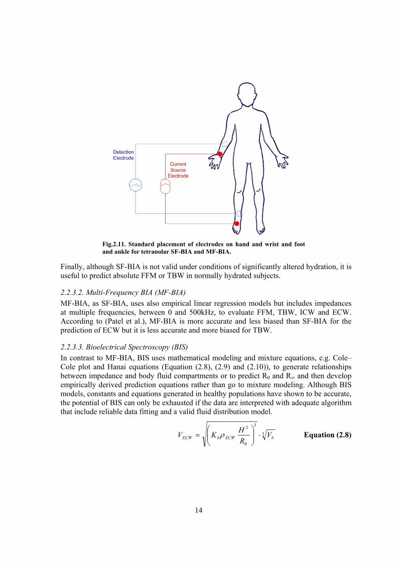
2.2.3.1. Single Frequency BIA (SF-BIA) A single frequency, generally at 50 kHz, is passed between surface electrodes placed on hand and foot (Fig.2.11). At 50 kHz BIA is not strictly measuring TBW but a weighted sum of ECW and ICW. SF-BIA permits to estimate FFM and TBW, but cannot determine differences in ICW and its results are based on a mixture theories and empirical equations.
Fig.2.10. Cylinder model for the relationship between the impedance and geometry.
14
Finally, although SF-BIA is not valid under conditions of significantly altered hydration, it is useful to predict absolute FFM or TBW in normally hydrated subjects.
2.2.3.2. Multi-Frequency BIA (MF-BIA) MF-BIA, as SF-BIA, uses also empirical linear regression models but includes impedances at multiple frequencies, between 0 and 500kHz, to evaluate FFM, TBW, ICW and ECW. According to (Patel et al.), MF-BIA is more accurate and less biased than SF-BIA for the prediction of ECW but it is less accurate and more biased for TBW.
2.2.3.3. Bioelectrical Spectroscopy (BIS) In contrast to MF-BIA, BIS uses mathematical modeling and mixture equations, e.g. Cole–Cole plot and Hanai equations (Equation (2.8), (2.9) and (2.10)), to generate relationships between impedance and body fluid compartments or to predict R0 and R∞ and then develop empirically derived prediction equations rather than go to mixture modeling. Although BIS models, constants and equations generated in healthy populations have shown to be accurate, the potential of BIS can only be exhausted if the data are interpreted with adequate algorithm that include reliable data fitting and a valid fluid distribution model.
3
3
0
2
bECWbECW VRHKV ⋅⎟⎟
⎠
⎞⎜⎜⎝
⎛= ρ Equation (2.8)
Fig.2.11. Standard placement of electrodes on hand and wrist and foot and ankle for tetrapolar SF-BIA and MF-BIA.
15
⎟⎟⎠
⎞⎜⎜⎝
⎛+=⎟⎟
⎠
⎞⎜⎜⎝
⎛+
∞ ECW
ICWb
ECW
ICW
VV
KRR
VV
11 05
2
Equation (2.9)
ECWICWTBW VVV += Equation (2.10)
Where Vx is the volume of the X-compartment, ρ is the resistivity, H is body height, Vb is body volume, R0 and R∞ are the Cole-resistances at low and high frequencies, respectively, and Kb is a dimensionless shape factor.
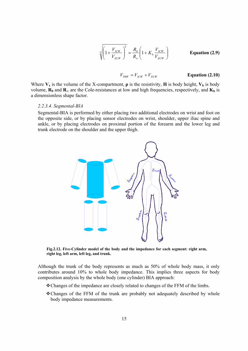
2.2.3.4. Segmental-BIA Segmental-BIA is performed by either placing two additional electrodes on wrist and foot on the opposite side, or by placing sensor electrodes on wrist, shoulder, upper iliac spine and ankle, or by placing electrodes on proximal portion of the forearm and the lower leg and trunk electrode on the shoulder and the upper thigh.
Although the trunk of the body represents as much as 50% of whole body mass, it only contributes around 10% to whole body impedance. This implies three aspects for body composition analysis by the whole body (one cylinder) BIA approach:
Changes of the impedance are closely related to changes of the FFM of the limbs.
Changes of the FFM of the trunk are probably not adequately described by whole body impedance measurements.
ZLeftArm
ZTrunk
Fig.2.12. Five-Cylinder model of the body and the impedance for each segment: right arm, right leg, left arm, left leg, and trunk.
16
Even large changes in the fluid volume within the abdominal cavity have only minor influence on the measurement of FFM or BCM.
2.2.3.5. Localized BIA Due to whole body BIA measures various body segments and is influenced by a several number of effects such as hydration, fat fraction or geometrical boundary conditions, the validity of simple empirical regression models is population-specific. Hence, to minimize the interference effects, Localized BIA, which focuses on well-defined body segments, is used.
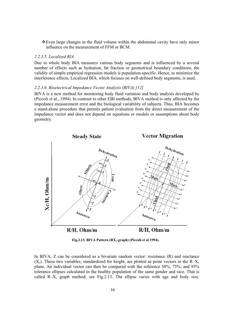
2.2.3.6. Bioelectrical Impedance Vector Analysis (BIVA) [12] BIVA is a new method for monitoring body fluid variation and body analysis developed by (Piccoli et al., 1994). In contrast to other EBI methods, BIVA method is only affected by the impedance measurement error and the biological variability of subjects. Thus, BIA becomes a stand-alone procedure that permits patient evaluation from the direct measurement of the impedance vector and does not depend on equations or models or assumptions about body geometry.
In BIVA, Z can be considered as a bivariate random vector: resistance (R) and reactance (Xc). These two variables, standardized for height, are plotted as point vectors in the R–Xc plane. An individual vector can then be compared with the reference 50%, 75%, and 95% tolerance ellipses calculated in the healthy population of the same gender and race. That is called R–Xc graph method; see Fig.2.13. The ellipse varies with age and body size.
Fig.2.13. BIVA Pattern (RXc-graph) (Piccoli et al 1994).
17
Furthermore, the following interpretations can be done when vector falls outside the 75% tolerance ellipse:
Vector displacements parallel to the major axis of tolerance ellipses indicate progressive changes in tissue hydration: dehydration with long vectors, out of the upper pole, and hyperhydration, or anasarca, with short vectors, out of the lower pole.
Vectors falling above (left) or below (right) the major axis of tolerance ellipses indicate more or less BCM, respectively, contained in lean body tissues.
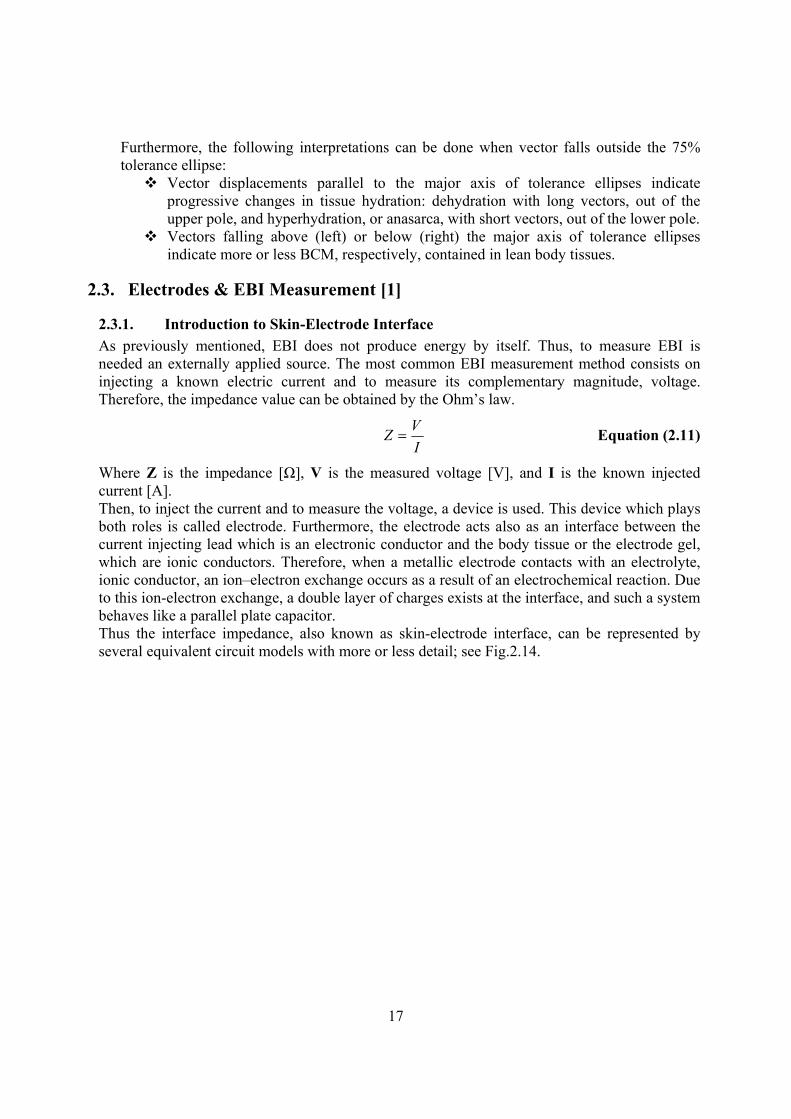
2.3. Electrodes & EBI Measurement [1]
2.3.1. Introduction to Skin-Electrode Interface As previously mentioned, EBI does not produce energy by itself. Thus, to measure EBI is needed an externally applied source. The most common EBI measurement method consists on injecting a known electric current and to measure its complementary magnitude, voltage. Therefore, the impedance value can be obtained by the Ohm’s law.
IVZ = Equation (2.11)
Where Z is the impedance [Ω], V is the measured voltage [V], and I is the known injected current [A]. Then, to inject the current and to measure the voltage, a device is used. This device which plays both roles is called electrode. Furthermore, the electrode acts also as an interface between the current injecting lead which is an electronic conductor and the body tissue or the electrode gel, which are ionic conductors. Therefore, when a metallic electrode contacts with an electrolyte, ionic conductor, an ion–electron exchange occurs as a result of an electrochemical reaction. Due to this ion-electron exchange, a double layer of charges exists at the interface, and such a system behaves like a parallel plate capacitor. Thus the interface impedance, also known as skin-electrode interface, can be represented by several equivalent circuit models with more or less detail; see Fig.2.14.
18
This impedance, Zep, is built up by the sweat and the electrode it-self and its value is typically unknown and frequency and time dependent.
2.3.2. EBI Measurement Configurations
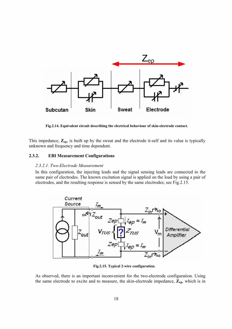
2.3.2.1. Two-Electrode Measurement In this configuration, the injecting leads and the signal sensing leads are connected to the same pair of electrodes. The known excitation signal is applied on the load by using a pair of electrodes, and the resulting response is sensed by the same electrodes; see Fig.2.15.
As observed, there is an important inconvenient for the two-electrode configuration. Using the same electrode to excite and to measure, the skin-electrode impedance, Zep, which is in
Fig.2.14. Equivalent circuit describing the electrical behaviour of skin-electrode contact.
Fig.2.15. Typical 2-wire configuration.
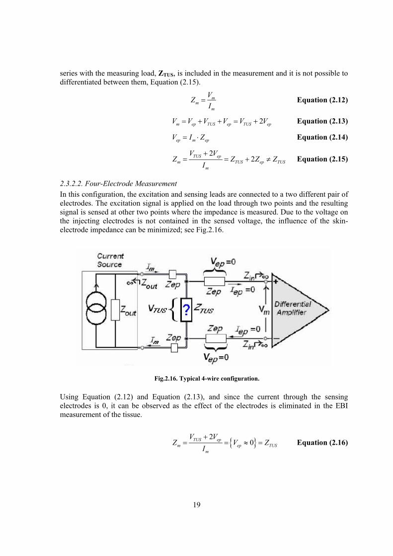
19
series with the measuring load, ZTUS, is included in the measurement and it is not possible to differentiated between them, Equation (2.15).
mm
m
VZI
= Equation (2.12)
2m ep TUS ep TUS epV V V V V V= + + = + Equation (2.13)
ep m epV I Z= ⋅ Equation (2.14)
22TUS ep
m TUS ep TUSm
V VZ Z Z Z
I+
= = + ≠ Equation (2.15)
2.3.2.2. Four-Electrode Measurement In this configuration, the excitation and sensing leads are connected to a two different pair of electrodes. The excitation signal is applied on the load through two points and the resulting signal is sensed at other two points where the impedance is measured. Due to the voltage on the injecting electrodes is not contained in the sensed voltage, the influence of the skin-electrode impedance can be minimized; see Fig.2.16.
Using Equation (2.12) and Equation (2.13), and since the current through the sensing electrodes is 0, it can be observed as the effect of the electrodes is eliminated in the EBI measurement of the tissue.
20TUS ep
m ep TUSm
V VZ V Z
I+
= = ≈ = Equation (2.16)
Fig.2.16. Typical 4-wire configuration.
20
2.4. Wearable Medical Devices [13]
2.4.1. Introduction to Wearable Medical Devices Nowadays the situation in many national health systems can be described as:
The life expectancy increases.
More chronic diseases are appearing, which need to be addressed as early as possible, in order to ensure optimal treatment, even cost-wise.
Medical advice is asked more often due to people become more health-conscious, but people do not want to spend more times at practices and hospitals.
The overall cost is ever increasing.
Because of all these issues, laboratory/hospital equipment are not enough and other kind of devices are needed. Wearable Medical Devices (WMDs) can offer a health and patient management system that support continuous monitoring, ubiquitous medical treatment and advice to patients at minimal cost. The idea behind WMDs is to make patients independent of their family doctor, to give them the opportunity to conduct simple measurements on their own and to actively participate in their health care.
2.4.2. Design Requirements & Challenges of WMDs As “Wearable” (and not only portable) means that the devices are so small and unobtrusive that they accompany the user to any place and any time, and due to achieve the previously mentioned idea, WMDs need to fulfill some design requeriments:
Small & Lightweight: Packaging overhead needs to be minimized due to volume/weight restrictions. Moreover, the WMD shall be unobtrusive in order to be worn as a daily accessory and should not look like a medical device.
Low power: A stand-alone power supply of minimum 15 hrs (= 1 working day) without recharging is mandatory. Apart from low-power components, also the duty cycle shall be used to optimize the power consumption of continuously operated equipment.
Housing: The device shall be shockproof, at least IP65, and biocompatible where exposed to the user. IP65 means according to International Protection Rating (IP), the device shows a complete protection against contact, even no ingress of dust, (range 6) and also shows a water protection against low pressure jets coming from any direction (range 5).
I/O interconnection: If a plug/socket option is selected, this adds mechanical issues and large, expensive hardware. On the other hand, if a wireless connection is selected, much larger power budget is required.
Sensors: Novel sensor concepts are required to be easily integrated into standard electronics or housings.
CHAPTER 3
SYSTEM DESIGN AND ITS IMPLEMENTATION
3.1. System Design Hardware
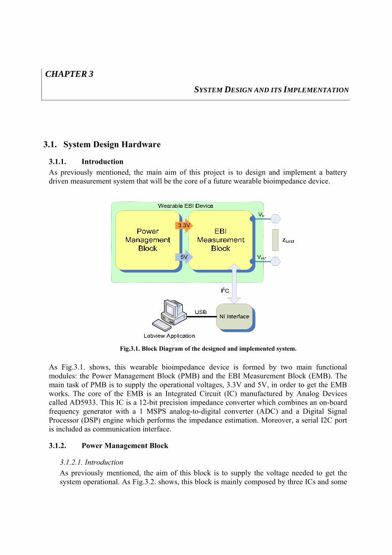
3.1.1. Introduction As previously mentioned, the main aim of this project is to design and implement a battery driven measurement system that will be the core of a future wearable bioimpedance device.
As Fig.3.1. shows, this wearable bioimpedance device is formed by two main functional modules: the Power Management Block (PMB) and the EBI Measurement Block (EMB). The main task of PMB is to supply the operational voltages, 3.3V and 5V, in order to get the EMB works. The core of the EMB is an Integrated Circuit (IC) manufactured by Analog Devices called AD5933. This IC is a 12-bit precision impedance converter which combines an on-board frequency generator with a 1 MSPS analog-to-digital converter (ADC) and a Digital Signal Processor (DSP) engine which performs the impedance estimation. Moreover, a serial I2C port is included as communication interface.
3.1.2. Power Management Block
3.1.2.1. Introduction As previously mentioned, the aim of this block is to supply the voltage needed to get the system operational. As Fig.3.2. shows, this block is mainly composed by three ICs and some
Fig.3.1. Block Diagram of the designed and implemented system.

22
basic electronic components such as resistances, capacitors or inductors. Using the Smart Power Selector from Maxim-IC, MAX8677A, the source to supply the system with power is selected. In this design, this supply can be provided by an AC Adapter or by a 1 cell Li-Po battery. Due to the System Supply Output (SYS) voltage varies depending on the input source, a Step-Up DC-DC Converter, MAX1763, is needed. Thus, a constant value of 5 DC-voltage is supplied to the rest of the system. Furthermore, using a Linear Regulator, LM1117, a 3.3 DC-voltage is also supplied.
3.1.2.2. MAX8677 The MAX8677A is available in a 4mm x 4mm, in a 24-pin TQFN-EP package. It works as an integrated 1-cell Li+ charger and Smart Power Selector™ with dual (DC and USB) power inputs. Furthermore, its main features are:
Complete Charger and Smart Power Selector. External MOSFETs are not required because of all power switches for charging and
switching the load between battery and external power are included on-chip. Can operate with either separate inputs for USB and AC adapter power, or from a
single input that accepts both. System operates with discharged or no battery. Automatic input selection switches the system load from battery to external power. Includes an input Overvoltage Protection (OVP) to 16V. 40mΩ System-to-Battery Switch. On-chip thermal regulation prevents overheating. Includes some indicators such as charge status and fault outputs, power-OK monitors,
charge timer, and battery thermistor monitor.
Fig.3.2. Power Management Scheme where all the components except of some capacitors are showed.

23
The Table 3-I shows the chief electrical characteristics extracted from its datasheet:
TABLE 3-I: MAX8677A ELECTRICAL SPECIFICATIONS.
PARAMETER MIN TYP MAX UNITS DC-TO-SYS PREREGULATOR
DC Operating Range 4.1 6.6 V DC Undervoltage Threshold 3.95 4.0 4.05 V DC Overvoltage Threshold 6.8 6.9 7.0 V
DC Supply Current 1 2 mA
DC-to-BAT Dropout Voltage 10 50 90 mV
DC Current Limit (RPSET = 1.5kΩ) 1800 2000 2200 mA PSET Resistance Range 1.5 6.3 kΩ SYS Regulation Voltage 5.1 5.3 5.5 V
VL Voltage 3.0 3.3 3.6 V
CHARGER
BAT-to-SYS On-Resistance 0.04 0.08 Ω
BAT Regulation Voltage 4.158 4.2 4.242 V
BAT Charge-Current Set Range 0.3 1.5 A ISET Voltage 0.9 1.0 1.1 V BAT Prequal Threshold 2.9 3 3.1 V
BAT Leakage Current 3 6 µA DONE Threshold as a Percentage of Fast-Charge (VTSET = open) 10 %
Maximum Prequal Time 30 Min
Maximum Fast-Charge Time 300 Min
LOGIC I/O: CHG, FLT, DONE, DOK, UOK, PEN1, PEN2, CEN, TSET, USUS
Logic Input Thresholds
High Level 1.3 V
Low Level 0.4
Hysteresis 50 mV
TSET Input Threshold
High Level VL – 0.3
V Midlevel 1.2 VL-1.2
Low level 0.3
Logic Input-Leakage Current 0.001 1 µA
*USB specifications are not showed because of USB input is not used in this system.

24
Paying attention to its blocks diagram, Fig.3.3., it can be observed the MAX8677A contains a Li-Po charger, as well as power MOSFETs and control circuitry to manage power flow. The Smart Power Selector circuitry offers flexible power distribution from an AC adapter or USB source to the battery (BAT) and system load (SYS). In our specific design, as the USB source input is cancelled, only the AC adapter source input (DC) supplies power. Therefore, if both an external power supply and battery are connected, the battery is charged with residual power from the DC input when the system load requirements are less than the input current limit. On the other hand, if both are connected but the system load requirements exceed the input current limit, the battery supplies supplemental current to the load. Finally, if there is no external supply connected, the system is powered from the battery.
Fig.3.3. MAX8677A Block Diagram. Due to the USB Power Management block is like DC Power Management block, this is not showed in detail.

25
The Input & Charger Current Limit Set Logic block controls the total SYS current, which is the sum of the system load current and the battery-charging current, through the logic inputs PEN1, PEN2 and USUS, and the analog inputs PSET and ISET; see Table 3-II.
NOT READY
TEMPERATURE SUSPENDICHG=0mA
UOK OR DOK = PREV. STATE
FLT = H.Z.CHG = H.Z.
DONE = H.Z.
ICHG=0mAUOK & DOK = H.Z.
FLT = H.Z.CHG = H.Z.
DONE = H.Z.
PREQUAL
ICHG=ICHGMAX/10
UOK OR DOK = LOW
FLT = H.Z.CHG = LOW
DONE = H.Z.0V≤VBATT≤3V
FAST CHARGE
ICHG≤ICHGMAX
UOK OR DOK = LOW
FLT = H.Z.CHG = LOW
DONE = H.Z.3V<VBATT<4.2V
TOP-OFF
ICHG<ITERM
UOK OR DOK = LOW
FLT = H.Z.CHG = H.Z.
DONE = H.Z.VBATT=4.2V
DONE
ICHG=0mA
UOK OR DOK = 0V
FLT = H.Z.CHG = H.Z.
DONE = LOW4.1V<VBATT<4.2V
FAULT
ICHG=0mA
UOK OR DOK = LOW
FLT = LOWCHG = H.Z.
DONE = H.Z.
ANY STATE
ANY CHARGING STATE
UOK OR DOK = LOWCEN = 0
VBATT < 2.8V
RESET TIMER
VBATT < 2.82VRESET TIMER RESET TIMER
VBATT > 3V
TOGGLE CENOR
REMOVE AND RECONNECTTHE INPUT SOURCES
CEN=HIGHOR
REMOVE AND RECONNECTTHE INPUT SOURCES
RESET TIMER
VBATT < 4.1V
RESET TIMERTIMER > 15s
TIMER > tPREQUAL
TIMER > tFASTCHARGE
TIMERRESUME.
THM OK
TIMERSUSPEND.
THM NOT OKICHG > ITERM
RESET TIMER
ICHG < ITERMAND VTERM=4.2V AND THERMAL OR INPUT LIMIT NOT EXCEEDED.RESET TIMER
Fig.3.4. MAX8677A Charger State Flowchart where H.Z. means High Impedance.

26
As in this design, the USB input is cancelled, the logic inputs PEN2 and USUS, which set the USB current limit, are not important. As PEN1 is always high, connected to VL, the DC input current limit is set by the value of RPSET. Thus, as RPSET is a fixed value of 1.5kΩ, a 2A DC input current limit is also set. Furthermore, ISET adjusts the maximum fast-charge current to match the capacity of the battery through a resistor, RISET. In this design a 1A value of maximum charge current is set by a value of 3kΩ of RISET. The battery charger initiates a charge cycle when the charger is enabled and there is a valid DC or USB input. See the charging state diagram illustrated in Fig.3.4. Firstly it detects the battery voltage and if it is less than the BAT prequal threshold (3.0V) then the charger enters into prequal mode, in which the battery charges at 10% of the maximum fast-charge current. This reduced charge rate ensures that the battery is not damaged by the fast-charge current while deeply discharged. Once the battery voltage rises to 3.0V, the charger transitions to fast-charge mode and applies the maximum charge current. Finally the battery voltage rises until it approaches the battery regulation voltage (4.2V). When charge current decreases to the value of fast-charge current set by TSET, 10% in this design, the charger enters a brief 15s top-off, and then charging stops. If the battery voltage subsequently drops below the 4.1V recharge threshold, charging restarts and the timers reset.
3.1.2.3. MAX1763 The MAX1763 is a high-efficiency, low-noise, step-up DC-DC converter proposed to use in battery-powered applications which require the longest possible battery life. Its main features are:
High Efficiency, usually up to 94%. It is possible to generate a fixed 3.3V Output or an Adjustable (2.5V to 5.5V) one from a wide range of input voltage (+0.7V to +5.5V).
Guarantees startup with an input voltage as low as 1.1V. The output voltage is generated by a 1MHz synchronous-rectified PWM boost topology with up to 1.5A output capability.
Includes an on-chip linear gain block to build an external linear regulator or a low-battery comparator.
Also includes a 1µA logic-controlled shutdown block and some soft-start and current limit functions to optimize the system.
Table 3-III shows some main electrical characteristics extracted from the MAX1763’s datasheet:
TABLE 3-II: INPUT LIMITER CONTROL LOGIC.
POWER SOURCE DOK UOK PEN1 PEN2 USUS DC INPUT CURRENT
LIMIT
MAXIMUM CHARGE
CURRENT AC Adapter at DC Input L X H X X 3000/RPSET 3000/RISET
DC and USB unconnected H H X X X No DC input 0

27
Although MAX1763 has 3 Operating Modes depending on the source connected to
TABLE 3-III: MAX1763 ELECTRICAL SPECIFICATIONS.
PARAMETER MIN TYP MAX UNITS DC-DC SWITCHES
POUT Leakage Current 0.1 10 µA LX Leakage Current 0.1 10 µA N-Channel Current Limit 2.0 2.5 3.4 A
P-Channel Current Limit 10 120 240 mA
REFERENCE
Reference Output Voltage 1.230 1.250 1.270 V Reference Supply Rejection 0.2 5 mV
GAIN BLOCK
AIN Reference Voltage 910 938 970 mV Transconductance 5 10 16 mS Gain Block Enable Threshold (VOUT-VAIN) 1.4 V Gain Block Disable Threshold (VOUT-VAIN) 0.2 V
DC CONVERTER
Input Voltage Range 0.7 5.5 V
Minimum Startup Voltage 0.9 1.1 V
Output Voltage 3.17 3.3 3.38 V FB Regulation Voltage 1.215 1.245 1.270 V FB Input Current (VFB = 1.35V) 0.01 100 nA
Output Voltage Adjust Range 2.5 5.5 V
Output Voltage Lockout Threshold 2.00 2.15 2.30 V
ISET Input Leakage Current 0.01 50 nA
No-Load Supply Current, Low-Power Mode 110 200 µA
LOGIC INPUTS
CLK/SEL Input High Level (0.8)
VOUT V
Low Level (0.2) VOUT
ONA and ONB Input High Level 1.6
V Low Level 0.4
Minimum CLK/SEL Pulse Width 100 ns
Maximum CLK/SEL Rise/Fall Time 100 ns
Logic Input-Leakage Current 0.01 1 µA

28
CLK/SEL input (logic 0, logic 1 or external clock), in this design only the Normal Operation can be selected (CLK/SEL = LOW); See Fig.3.5.
During DC-DC converter operation, the internal N-channel MOSFET switch turns on for the first part of each cycle, allowing current to ramp up in the inductor (L1) and store energy in a magnetic field. During the second part of each cycle, the MOSFET turns off and inductor current flows through the synchronous rectifier to the output filter capacitor and the load. As the energy stored in the inductor is depleted, the current ramps down and the synchronous rectifier turns off, the N-channel FET turns on and the cycle repeats. With small loads, depending on the operating mode, the output voltage is regulated using either PWM or by switching only as needed to service the load. In its normal mode of operation, the MAX1763 operates in PWM when driving medium to high loads and at light loads it only switches as needed. This optimizes efficiency over the widest range of load conditions. It offers fixed-frequency PWM operation through most of its load range. Furthermore, in this design, an external Schottky diode (D1) must be connected from LX to POUT pin because the output voltage is greater than 4V (VPOUT = 5V). To reach this output voltage value, a resistor voltage-divider to FB from OUT to GND is needed. Thus, accordingly with the device’s datasheet (Equation (3.1)), the values of R1 and R2 are chosen:
2
51.24530 1
1 22
821
27
OUT
FB
VV V
R kOUT
FB
R kVR RR kV
=⎧ ⎫⎪ ⎪=⎨ ⎬⎪ ⎪≤ Ω⎩ ⎭
= Ω⎛ ⎞= − ⎯⎯⎯⎯⎯→⎜ ⎟ = Ω⎝ ⎠
Equation (3.1)
Fig.3.5. MAX1763 Block Diagram using the Normal-Mode Operation and setting the Output Voltage at 5V.

29
3.1.3. EBI Block
3.1.3.1. Introduction As previously mentioned and it is also showed in Fig.3.6, the core of this block is the IC called AD5933.
As showed, 5V are supplied by the Power Management Block. Furthermore, the I2C module is connected to a National Instrument (NI) Device to configure the AD5933. Thus, the IC estimates the load between Vin and Vout pins and the result is sent by the I2C module to a Labview application though the NI Device.
3.1.3.2. AD5933 This IC is a high precision impedance converter system composed by several blocks, as illustrated Fig.3.7. In the exciting channel, sine waveforms are generated digitally by a 27-bit Direct Digital Synthesizer (DDS); see Fig.3.8 to know as the DDS works. The clock of this DDS is generated by either an external clock which is connected to the MCLK pin or by an internal clock. Thus, once the analog waveform is generated, it is amplified through a programmable gain stage and a programmable voltage output excitation is set up. Although there are four different ranges, in this design it is only used Range 1. In this range, the output excitation voltage amplitude and the output DC Bias level are, respectively, 1.98 Vp-p and 1.48 V. Later, this output excitation signal at a particular frequency is applied to the measuring load, which is connected between VOUT and VIN pins. Therefore, as a response to this excitation voltage, a current is flowing through the working impedance and it is acquired by the Response channel. This stage is a current sensing stage and it is composed by a current-to-voltage amplifier followed by a programmable gain amplifier (PGA), an antialiasing filter, and an ADC. Thus, the current flowing through the unknown impedance becomes a voltage signal at the output of the current-to-voltage converter. The gain of this current-to-voltage
Fig.3.6. EBI Block without any capacitors.

30
amplifier is chosen by the user connecting a feedback resistance between RFB and VIN pins. It is very important to maintain the signal within the linear range of the ADC (0V to VDD). To get this, both the feedback resistance and the PGA gain must be calculated following the Equation (3.2).
Gain Setting resistorGain Output Excitation Voltage PGA GainZunknown
= × × Equation (3.2)
Finally, the digital data from the ADC is passed to the DSP core and the DFT is performed. The DFT algorithm used in AD5933 consists on a multiplication which is accumulated over 1024 samples for each frequency point; see Equation (3.3). The result of this DFT is stored in twos complement format in two, 16-bit registers: the real and the imaginary registers.
( ) ( ) ( ) ( )( )( )1023
0cos sin
nX f x n n j n
=
= −∑ Equation (3.3)
Where X(f) is the power in the signal at the Frequency Point f, x(n) is the ADC output, cos(n) and sin(n) are the sampled test vectors provided by the DDS core at the Frequency Point f, and j is the imaginary value -1 .
As observed, this IC is quite complete and its registers have not been showed yet. In the next section, a Labview software, which configures these registers and uses the stored data, is presented. But before that, some main electrical specifications are shown in the Table 3-IV.
Transmit Stage
DFTReceive Stage
DDSCORE
(27 BITS)DAC
TEMPERATURESENSOR
OSC
I2C INTERFACEµC
LPFADC
WINDOWINGOF DATA
+-
cos sinIMAGREGISTER
MAC CORE(1024 DFT)
REALREGISTER
MCLK
VDD/2+-
ROUT
SCL
SDA
MCLK
VOUT
RFB
Z(ω)
VINx5x1
AD5933
VBIAS
R(GAIN)
Fig.3.7. AD5933 Functional Block Diagram. There are 3 main blocks: Transmit and Receive Stages and DFT.

31
TABLE 3-IV: AD5933 ELECTRICAL SPECIFICATIONS.
PARAMETER MIN TYP MAX UNITS SYSTEM
Impedance Range 1k 10M Ω Total System Accuracy 0.5 %
TRANSMIT STAGE
Output Frequency Range 1 100 kHz
Output Frequency Resolution 0.1 Hz
MCLK Frequency 16.776 MHz
TRANSMIT OUTPUT VOLTAGE (Range 1)
AC Output Excitation Voltage 1.98 Vp-p DC Bias 1.48 V DC Output Impedance 200 Ω
RECEIVE STAGE
Input Leakage Current 1 nA
Input Capacitance 0.01 pF
Feedback Capacitance 3 pF
ANALOG-TO-DIGITAL CONVERTER
Resolution 12 Bits
Sampling Rate 250 kSPS
POWER REQUIREMENTS
VDD 2.7 5.5 V
IDD Normal mode 10 15 mA Standby mode 11 Power-Down mode 0.7 5 µA
LOGIC INPUTS
Input Voltage High Level 0.7 x VDD
V Low Level 0.3 x VDD

32
3.1.4. Implementation Board This wearable EBI device has been designed using a software called OrCAD. It is a proprietary software tool suite used primarily for electronic design automation. Therefore, it is used mainly to create electronic prints for manufacturing of printed circuit boards. Furthermore, this software also allows to create electronic schematics and diagrams being able to simulate them. Once the PCB has been design through the OrCAD Layout Application, the final board has been manufactured out of the university by an external company. The main reason to do this has been because of almost all components have been chosen in SMD packages to reduce the size and the weight of the final board as soon as possible. Thus, the final board is showed in Fig.3.9. and it can be observed as all components have been placed on the top and the battery on the bottom.
Fig.3.8. DDS Block Diagram. The Sampled Sine Wave is obtained through an angle to amplitude converter which transforms the truncated phase into an amplitude value. [14]

33
3.2. Software Implementation
3.2.1. Introduction As previously mentioned, the AD5933 has an I2C interface. Through this, AD5933 is configured with the desired parameters to estimate the impedance and later, this result can be sent by the I2C interface to other application to be processed or evaluated. As it will be explained in the next sub-section, the I2C protocol is a Master-Slave communication. In our design, the AD5933 acts as a Slave and as a Master, the NI I2C/SPI Interface called USB-8451 has been chosen. This device allows to connect to and to communicate with I2C, SMBus, and SPI devices. Furthermore, it is a good solution to communicate with consumer electronics such as PCs or Laptops due to its plug-and-play USB connection. Thus, using this device, the implemented board is connected to a PC where runs a Labview application.
Fig.3.9. Final Board Top Layer.
Fig.3.10. NI USB-8451 device.

34
3.2.2. I2C Protocol [15] [16] [17]
3.2.2.1. I2C Introduction I2C is a multi-master serial computer bus invented by Philips and it is used to attach low-speed peripherals to a motherboard or an embedded system. I2C has only two bi-directional lines called Serial Data (SDA) and Serial Clock (SCL) to carry information between the devices. Due to the fact that there is only a unique line for data, the I2C is a half-duplex system; a device cannot receive and send data at the same time. Each device is usually recognized by a unique 7-bit address, although a 10-bit address is also possible. Furthermore, I2C devices can operate as Master or Slave. The main tasks of a Master device are to generate and control the clock signal, to start and stop the data transfer process and to control addressing of other devices. The Slave device is the one that is addressed by the Master. Furthermore, both of them, Master and Slave, act as Transmitter and Receiver in two common mode of operation: a Master-transmitter sends data to a Slave-receiver or a Master-receiver requires data from a Slave-transmitter.
Depending on the speed which the data are transferred, there are three modes: Standard Mode (100kbps), Fast Mode (400kbps) and High Speed Mode (3.4Mbps). About the maximum number of devices which can be connected together, it is limited by the address space and also by the total bus capacitance of 400 pF.
3.2.2.2. I2C Bus Characteristics Depending on the state of both SDA and SCL lines, during a communication the following scenarios can occur:
Idle State: This situation happens when the I2C bus is not busy and both lines remain high due to the pull-up resistors. It can be observed that after a Stop Condition (P) and before next Start Condition (S).
Vdd
Rp Rp
SDASCL
OUT
INININ IN
OUT OUTOUT
DEVICE 2DEVICE 1 Fig.3.11. Typical I2C connection. The device outputs are wired with signal on bus.

35
Start Condition (S): This situation occurs during a High to Low transition of SDA line while the SCL remains high.
Stop Condition (P): It is a Low to High Transition of SDA line while SCL remains high.
Data Valid: Data are valid when the SCL is high. Data must be stable during high clocks and it can change only during low clocks. Every data bit is only interpreted per one clock pulse. If any change occurs in SDA while SCL is high, it will be interpreted as S or P condition.
Acknowledge (ACK): Each device generates an ACK signal after the reception of each byte. The master generates an extra clock pulse and if the device pulls down the SDA line, an ACK is interpreted. On the other hand, if SDA is high, a Not-ACK (NACK) is interpreted.
3.2.2.3. I2C Protocol I2C follows a master/slave protocol. The master is the device which always initiates the communication. For it, the master sends a start condition which informs all the slave devices to listen for instructions on the SDA. After that, the master sends the 7-bit address of the target slave and a read/write flag (low logic level to write to the slave and high logic level to read from the slave). If the slave with the matching address exists, it responds with an ACK. Thus, the communication proceeds between the master and the slave on SDA. Both the master and slave can receive or transmit data depending of the flag value. The transmitter sends 8-bits of data to the receiver which replies with a 1-bit acknowledgement when it receives the byte. Finally, when the communication is complete, the master sends a stop condition indicating that everything is done.
Fig.3.12. Timing Diagram.
Fig.3.13. I2C generic Protocol. First, Master sends start (S), slave address and R/W flag and Slave answers an ACK. Later, Transmitter is sending 1-byte data and Receiver is answering with an ACK. Finally, Master sends a Stop Condition (P) to indicate the communication is over.

36
3.2.3. Labview Application
3.2.3.1. Introduction Our designed board is connected to a PC running a Labview application by the NI I2C/SPI Interface. Labview is a platform and development environment for a visual programming language, called “G”, created by National Instruments. It is used by scientists and engineers for several tasks such as data acquisition, automated test and instrument control, industrial measurements and control, and embedded design. As Labview is a visual programming language, there is no need to write any code. A Labview program consists of a several linked blocks known as Virtual Instruments, VIs. Through the designed application, it is allowed to configure the AD5933 and to process the data stored in real and imaginary registers. In the next sub-sections, all of the Vis designed in this project are showed and explained.
3.2.3.2. AD5933 Configuration Blocks The AD5933 permits the user to perform some features before estimation is made. To configure these user-defined parameters, a new VI, called FreqMeas, has been created. This VI has seven inputs and four outputs; see Fig.3.14.
Through this VI, the user can define the start frequency (Frequency), the frequency resolution (Frequency Increment), and number of points in the frequency sweep (Increments). Furthermore, the value of the clock (MCLK) and the number of settling time cycles (Setting Time Cyles), which determines the number of output excitation cycles can pass through the unknown impedance before ADC conversion starts, must be added. The other two inputs are used to indicate that the NI-845 is the master device and to configure the speed and addressing, 7-bit address in this case, in the I2C protocol. Moreover, AD5933 address is also indicated as 0x0D in hexadecimal or 0b0001101. As noticed, only 7 bits are
Fig.3.14. FreqMeas VI. Its 7 inputs and only 2 outputs are showed.

37
used to indicate the slave address due to 8th bit, LSB, is used as a Read or Write flag and it is the NI-845 software which internally sets this bit to the correct value. Finally, the outputs called Real and Imaginary show the value which is stored in these registers. Before explaining this VI in more detail, the Table 3-V shows the AD5933 Register Map.
To explain in detail this VI, it is easier to show all the steps through a flowchart; see Fig.3.15. The first Stage in the flowchart represents the four frames at the beginning of the VI Sequence. The values of the Start Frequency and the Frequency Increment are calculated following, respectively, the Equation (3.4) and the Equation (3.5).
27Required Output Start Frequency 2
4
Start Frequency CodeMCLK
⎛ ⎞⎜ ⎟⎜ ⎟= ×
⎛ ⎞⎜ ⎟⎜ ⎟⎜ ⎟⎝ ⎠⎝ ⎠
Equation (3.4)
27Required Frequency Increment 2
4
Frequency Increment CodeMCLK
⎛ ⎞⎜ ⎟⎜ ⎟= ×
⎛ ⎞⎜ ⎟⎜ ⎟⎜ ⎟⎝ ⎠⎝ ⎠
Equation (3.5)
TABLE 3-V: AD5933 REGISTER MAP.
Name Register
Control High (D15 to D8) 0x80 Low (D7 to D0) 0x81
Start Frequency High (D23 to D16) 0x82 Middle (D15 to D8) 0x83 Low (D7 to D0) 0x84
Frequency Increment High (D23 to D16) 0x85 Middle (D15 to D8) 0x86 Low (D7 to D0) 0x87
Number of Increments High (D15 to D8) 0x88 Low (D7 to D0) 0x89
Number of Settling Time Cycles High (D15 to D8) 0x8A Low (D7 to D0) 0x8B
Status D7 to D0 0x8F
Real Data High (D15 to D8) 0x94 Low (D7 to D0) 0x95
Imaginary Data High (D15 to D8) 0x96 Low (D7 to D0) 0x97

38
Later, these values and the values of the Number of Increments and the Number of Settling Time Cycles are split in 1-byte blocks and stored in their relevant registers. Although the number of settling time cycles can be increased by a factor of 2 or 4 depending upon the status of the bits D10 and D9, in this design this increase factor is not used. Thus, the value stored in the register 0x8A must not be changed. In the second stage, AD5933 is placed into Standby Mode writing in the High Control Register (0x80) the value 0xB0. Due to Control Register and Status Register are often used, they are shown in the Table 3-VI.
In the third stage, firstly AD5933 is configured to use the internal system clock, a PGA gain factor of x1 and an excitation voltage of 2.0Vp-p typical (Range 1). Thus, a value of 0x00 and a value of 0x01 are written in the Low and High Control Registers, respectively. Finally, AD5933 is programmed with a Initialize with Start Frequency command (value 0x10 in High Control Register). In the next stage, after a constant delay has elapsed, a Start Frequency Sweep command (0x20) is write in the High Control Register. Then, after waiting a sufficient amount of time, which has been calculated depending on the number of settling time cycles and the value of the frequency, the Status register is polled to check if the DFT conversion is complete. To check this, a value of 0x02 must be stored in the Status register.
TABLE 3-VI: CONTROL & STATUS REGISTER MAP.
Control Register
Con
trol
Reg
iste
r
Hig
h R
egis
ter
Bit Function Bit Function D15 D14 D13 D12 D11 D10 D9 D8
0 0 0 1 Initialize with start frequency x 0 0 x 2.0 Vp-p typical
0 0 1 0 Start frequency sweep x 0 1 x 200 mVp-p
typical
0 0 1 1 Increment frequency x 1 0 x 400 mVp-p
typical 0 1 0 0 Repeat frequency x 1 1 x 1.0 Vp-p typical
1 0 0 1 Measure temperature x x x 0 PGA gain x5
1 0 1 0 Power-down mode x x x 1 PGA gain x1 1 0 1 1 Standby mode
Low
R
egis
ter
Bit Function
Bit Function
D7 D6 D5 D4 D3 D2 D1 D0 0 0 0 0 No Reset 0 0 0 0 Internal clock 0 0 0 1 Reset 1 0 0 0 External clock
Status Register
Stat
us
Reg
iste
r D7 D6 D5 D4 D3 D2 D1 D0 Function 0 0 0 0 0 0 0 1 Valid Temperature measurement 0 0 0 0 0 0 1 0 Valid Real/Imaginary Data 0 0 0 0 0 1 0 0 Frequency sweep Complete

39
When the DFT is complete, the values of the Real and Imaginary registers are read. Due to both of these values are stored in 16-bit, twos complement format, they must be decoded. In the final stage, AD5933 is programmed into Power-down mode. This stage is implemented out of the FreqMeas VI.
3.2.3.3. Impedance Magnitude Calculation After reading values from Real and Imaginary Data registers, the magnitude is calculated by the Equation (3.6).
22 IRMagnitude += Equation (3.6)
Where R is the real number stored in High and Low Real registers, and I is the imaginary value stored in High and Low Imaginary registers. But this value is not the real estimated value of the impedance magnitude, to obtain it this value must be multiplied by a gain factor which is calculated during the calibration. To obtain this gain factor, a calibration impedance is connected between VIN and VOUT pins. Thus, after calculating the DFT magnitude at a certain frequency point, the Gain factor is obtained by the Equation (3.7).
1calibration Impedance
Gain Factor Magnitude
⎛ ⎞⎜ ⎟⎝ ⎠= Equation (3.7)
Program Frequency Sweep Parameters into
(1) Start Frequency Register(2) Number of Increments Register(3) Frequency Increment Register(4) Number of Settling Time Cycles
Place the AD5933 into Standby Mode
Program Initialize with Start Frequency Command to the
Control Register
After a Delay, Program Start Frequency Sweep Command in the
Control Register
After a sufficient amount of Settling Time has elapsed, Poll the Status
Register to check if the DFT conversion is complete
NO
Read Values From Real and Imaginary Data Registers
YES Program the AD5933 into Power-Down Mode
Fig.3.15. AD5933 Frequency Sweep Flowchart.

40
Due to the fact that the gain factor is frequency-dependent, to minimize the error, in this design the gain factor points are calculated at every single frequency that the impedance will be measured and they are stored in an array. Later, this array is used to compensate the time delay introduced by the circuitry and accurately estimate the true value of the working load impedance. This value is obtained in the same way as the gain factor but using a unknown load instead; see Fig.3.16. Thus, the measured impedance at frequency point is given by the Equation (3.8).
MagnitudeFactorGain ×=
1 Impedance Equation (3.8)
Fig.3.16. AD5933 Calibration and Impedance Magnitude Blocks.

41
3.2.3.4. Impedance Phase Calculation As AD5933 stores the real and imaginary values in different registers, the phase across an unknown impedance can be measured according to the Equation (3.9).
( )RI1tan)Phase(rads −= Equation (3.9)
Where tan-1 is the arctangent, I is the imaginary value stored in High and Low Imaginary registers, and R is the real component stored at High and Low Real registers. As well as in impedance magnitude calculation, a calibration is required due to the AD5933 system phase is added in the measure. Thus, the first step to measure the phase of an unknown impedance consists of measuring the phase, Equation (3.9), placing a resistor between VIN and VOUT pins. Due to the phase of a resistor is zero, the measured phase depends entirely on the AD5933 system. Once the system phase has been calculated for every certain frequency point and these values have been stored in an array, the phase of an unknown impedance is calculated using the Equation (3.10). Due to the Equation (3.9) is only working on the range between –π/2 and π/2 and the correct phase depends on the sign of the real and imaginary component, several conditions are used in the Matlab script, which is used in this application, and are summarized in the Table 3-VII.
systemunknownZ ∇−Φ=θ Equation (3.10)
Where ∇ system is the phase of the system, and Фunknown is the phase of the system and the unknown impedance. Both of these phases are calculated through the Equations summarized in the Table 3-VII. Finally Zθ is the phase due to the unknown impedance.
TABLE 3-VII: PHASE ANGLE.
Quadrant Real Imaginary Phase Angle (degrees)
1st + + ( )π
01 180tan ×−
RI
2nd - + ( )π
010 180tan180 ×+ −
RI
3rd - - ( )π
010 180tan180 ×+ −
RI
4th + - ( )π
010 180tan360 ×+ −
RI

CHAPTER 4
MEASUREMENTS AND VALIDATION
4.1. Board Electrical Characteristics
4.1.1. Battery Life To check the battery life time, the system has been tested in two different operation modes. The first one is simulating a Standby mode. No measurements have been taken during the time which the battery voltage has been acquired. The other operation mode is completely the opposite situation, with the system working in Continuous Acquisition mode. In this mode, a sample is measured per second. Since the operation modes are the opposite of each other the battery time of any other operation mode between these two can be extrapolated. As it is shown in Fig.4.1, the battery life in Standby mode is around 61520 seconds, equivalent to 17 hours 5 minutes and 20 seconds. On the other hand, in the Continuous Acquisition mode, the battery life is around 43570 seconds, or 12 hours 6 minutes and 10 seconds.
Fig.4.1. Graph of the Battery Life operating in 2 modes: in standby mode (blue) and acquiring 1 sample per second (red).

43
4.2. EBI Measurements
4.2.1. Resistance Measurements To check the operational dynamic frequency range of the system, several known values of resistances have been tested. The chosen frequency range is the β-dispersion range, from around 10 kHz to 100 kHz. The main reasons are due to the limitation of the AD5933 to measure values below 5 kHz and also because of the most interesting dispersion in medical applications is β-dispersion, as mentioned in Chapter 2. Thus, two decades of resistance values, from 100Ω to 10kΩ, have been tested in 5 kHz-frequency steps after calibrating the system with a resistance value of 5100Ω. Table 4-I shows some of the obtained measurement values.
In Fig.4.2 an ‘Estimated resistance vs. frequency’ graph is shown. As it can be observed, every plot for every resistance value is completely flat, i.e constant. That means the estimated values, which have been acquired by the system, are independent on the frequency as expected from theory. On the other hand, some problems can be observed. Firstly, for very low values of resistance the device exhibits a high error due to the design is not very accurate in this load range. Secondly, values below calibration resistance show a positive offset and values above calibration show a
TABLE 4-I: MEASUREMENTS OF DIFFERENT RESISTANCES FOR SEVERAL FREQUENCIES.
Rth (Ω) Frequency (Hz)
5000 10000 20000 40000 60000 80000 100000 100 475 478 478 473 469 465 459 150 492 494 495 490 487 485 480 270 551 554 556 553 548 545 542 360 600 603 605 599 596 591 592 430 640 643 646 642 638 636 633 510 705 710 712 710 710 712 712 620 818 823 826 824 824 825 825 750 930 936 939 937 936 937 936 820 1004 1009 1013 1010 1010 1010 1010 1000 1163 1170 1174 1171 1170 1171 1169 2200 2275 2283 2289 2284 2282 2284 2282 2700 2788 2795 2802 2794 2796 2792 2795 3300 3343 3357 3357 3357 3352 3352 3350 4300 4276 4298 4300 4292 4293 4283 4293 5100 5095 5101 5104 5109 5102 5103 5089 6200 6137 6154 6152 6129 6143 6142 6150 7500 7417 7365 7353 7349 7376 7388 7362 8200 7988 7946 7936 7916 7961 7925 7961 9100 8898 8902 8831 8841 8882 8885 8881
10000 9698 9715 9671 9729 9738 9683 9722

44
negative one. This can be better observed in the Fig.4.3 where an ‘expected value vs. theoretical value’ plot is shown for several frequencies.
Except at high values, a frequency-independence is observed along the tested range. Due to this fact, a software calibration is proposed to improve the results; see Fig.4.4. This software calibration consists on applying the Equation (4.1). This equation is obtained calculating a regression line in the range between 500 Ω and 10kΩ at the frequency of 50 kHz.
( ) 9494.066.228cal −= ZmeasZ Equation (4.1)
Where Zmeas is the value obtained from AD5933 and Zcal is the calculated value applying the software calibration.
Fig.4.2. Resistance value vs. Frequency plot. Several resistances have been tested for the frequency range between 100Hz and 10 kHz in 5kHz-frequency steps.

45
Table 4-II contains the compensated values for the same resistances and frequencies used in Table 4-I.
Fig.4.3. Theoretical Resistance vs. Measured Resistance for several frequencies: 5kHz, 25kHz, 50kHz, 75kHz and 100kHz. As observed, a frequency-dependence does not exist except of high values.
Fig.4.4. Software Calibration Block.

46
Table 4-III contains the errors with and without applying the calibration at 50 kHz are shown. As noticed, there is a high improvement using this calibration.
TABLE 4-II: ACQUIRED VALUES APPLYING THE SOFTWARE CALIBRATION.
Rth (Ω) Frequency (Hz)
5000 10000 20000 40000 60000 80000 100000 100 259,47 262,63 262,63 257,36 253,15 248,94 242,62 150 277,38 279,48 280,54 275,27 272,11 270,00 264,74 270 339,52 342,68 344,79 341,63 336,36 333,20 330,04 360 391,13 394,29 396,40 390,08 386,92 381,65 382,70 430 433,26 436,42 439,58 435,37 431,16 429,05 425,89 510 501,73 506,99 509,10 506,99 506,99 509,10 509,10 620 620,75 626,02 629,18 627,07 627,07 628,12 628,12 750 738,72 745,04 748,20 746,09 745,04 746,09 745,04 820 816,66 821,93 826,14 822,98 822,98 822,98 822,98
1000 984,14 991,51 995,72 992,56 991,51 992,56 990,46 2200 2155,40 2163,83 2170,15 2164,88 2162,78 2164,88 2162,78 2700 2695,74 2703,12 2710,49 2702,06 2704,17 2699,96 2703,12 3300 3280,32 3295,07 3295,07 3295,07 3289,80 3289,80 3287,70 4300 4263,05 4286,22 4288,33 4279,90 4280,96 4270,42 4280,96 5100 5125,70 5132,02 5135,18 5140,45 5133,07 5134,13 5119,38 6200 6223,24 6241,14 6239,04 6214,81 6229,56 6228,50 6236,93 7500 7571,46 7516,68 7504,04 7499,83 7528,27 7540,91 7513,52 8200 8172,89 8128,65 8118,12 8097,05 8144,45 8106,53 8144,45 9100 9131,39 9135,60 9060,82 9071,35 9114,54 9117,70 9113,48 10000 9974,03 9991,93 9945,59 10006,68 10016,16 9958,23 9999,30
TABLE 4-III: ERROR WITH AND WITHOUT APPLYING THE SOFTWARE CALIBRATION AT 50 KHZ.
Rth (Ω) Error (Zmeas-Rth)
Rth (Ω)Error (Zmeas-Rth)
Without Calibration Calibration Without Calibration Calibration100 373 157,36 2200 87 -31,96 150 340 125,27 2700 99 7,33 270 282 70,57 3300 55 -7,04 360 240 31,13 4300 -6 -17,99 430 213 6,42 5100 5 36,23 510 202 -0,90 6200 -51 35,88 620 206 9,18 7500 -123 29,32 750 189 -1,80 8200 -240 -56,60 820 192 5,09 9100 -233 -1,26 1000 173 -5,33 10000 -278 -0,70

47
4.2.2. RC Circuit Topology Measurements Two different circuit topologies have been chosen to test the performance of the measurement system obtaining the frequency response of a test load. In both cases, its phase and its magnitude were acquired and compared with the theoretical data, after applying the software calibration. As observed, the error in the measured phase is increased along the frequency reaching a maximum value of 5 degrees; see Fig.4.7 and Fig.4.9. On the other hand, the measured magnitude only shows a little error for small values of the frequency range; see Fig.4.6 and Fig.4.8. The chosen topologies have been previously explained in Chapter 2 and they correspond with Fig.2.6 and Fig.2.4(c).
y = 0,9494x + 228,66R2 = 0,9999
0
2000
4000
6000
8000
10000
12000
0 1000 2000 3000 4000 5000 6000 7000 8000 9000 10000
Rth
Res
t
Range 500<R<10k Linear (Range 500<R<10k)
Fig.4.5. Tendency Line using a linear regression in the range between 500Ω and 10kΩ.

48
R1=1 kΩ
R2=7.5 kΩ
C=1 nF
Fig.4.6. Impedance Magnitude vs. Frequency for a R1+R2//C topology. It corresponds with the topology shown in Fig.2.6 with R1=1k, R2=7k5 and C=1nF.
R1=1 kΩ
R2=7.5 kΩ
C=1 nF
Fig.4.7. Impedance Phase vs. Frequency for a R1+R2//C topology. It corresponds with the topology shown in Fig.2.6 with R1=1k, R2=7k5 and C=1nF.

49
Re=7.5 kΩ
C=1 nF Ri=1.2 kΩ
Fig.4.8. Impedance Magnitude vs. Frequency for a Re//(Ri+C) topology. It corresponds with the topology shown in Fig.2.4(c) with Re=7k5, Ri=1k2 and C=1nF.
Fig.4.9. Impedance Phase vs. Frequency for a Re//(Ri+C) topology. It corresponds with the topology shown in Fig.2.4(c) with Re=7k5, Ri=1k2 and C=1nF.

50
4.2.3. Biological Measurements To test the performance of the system measuring EBI, two kinds of measurements were taken. In thr first measurement, the EBI of a banana was measured along the frequency range between 5kHz and 100kHz. Both the obtained magnitude and phase are shown in Fig.4.10 (a) and (b), respectively. Since it is not possible to acquire data below 5kHz using the AD5933 without using a frequency divider, the magnitude plot starts in the slope and the maximum value cannot
be observed. On the other hand, the phase plot shows how the minimum value is reached. The second measurement consists on impedance pneumography. This method is used as a method for monitoring breathing. It consists on placing a surface electrode in each side of the thorax and measuring the variation of the impedance during inspirations and expirations. Usually and depending on the subject, on a base impedance of about 200 Ω, variations in the range of 2 Ω to 6 Ω can be observed in peak-to-peak amplitude for normal breathing. [18] [19]
Fig.4.10. (a) Magnitude of a banana EBI along the β-dispersion range. (b) Phase of a banana EBI along the β-dispersion range. The start frequency is 5 kHz.

51
Fig.4.11 shows an impedance pneumography acquired by the designed system. For safety reasons, these measurements were acquired using batteries as power sources to guarantee the isolation. In the figure, it can be observed as the base impedance is upper than 200 Ω and the peak-to peak amplitude is around 4 Ω as expected. The base impedance is higher due to our system is configured as a two-electrode system and the influence of the skin-electrode cannot be minimized as mentioned in Chapter 2.
4.3. Measurement Validation
4.3.1. Noise Influence in Measurements To check how the measurements are influenced by noise, 500 samples of three different values of resistances (820Ω, 5100Ω and 8200Ω) were acquired for 2 different frequencies, 5kHz and
Fig.4.11. Impedance Pneumography. It shows a base impedance of 264.4 Ω and a peak-to-peak amplitude around 4 Ω.

52
100kHz. Thus, applying the Matlab function called histfit(), an histogram with superimposed normal density is plotted for each data array; see Fig.4.12.
Assuming that data act as a normal distribution, the made error is measured in the interval [μ-kσ, μ+kσ] where μ is the mean value of the data array, σ is the standard deviation of the data array and k is chosen for a p-value of 0.01 (k = 2.6); see Table 4-IV.
Fig.4.12. 500-sample histogram of several resistance values at two different frequencies. (a) Resistance of 820 Ω at 5 kHz. (b) Resistance of 5100 Ω at 5 kHz. (c) Resistance of 8200 Ω at 5 kHz. (d) Resistance of 820 Ω at 100 kHz. (e) Resistance of 5100 Ω at 100 kHz. (f) Resistance of 8200 Ω at 100 kHz.

53
Thus, as the Table 4-IV shows, it can be assumed the measurements are not influenced severely by noise.
4.3.2. Temperature Influence in Measurements To study the influence of the temperature, measurements on a carbon-film resistance with a reference value of 1kΩ were acquired during a period of time while the temperature changes approximately for 1ºC. Fig.4.15 shows a slight slope with a linear tendency. It can be observe a deviation of -0.86 Ω/ºC (or 860 ppm/ºC). Since this deviation is within the typical temperature coefficient range for this kind of resistances i.e. 1200 ppm/ºC, it can be concluded that the measurements acquired by the system are not significantly influenced by the temperature. Nevertheless, there is an apparent delay of 4 hours between the temperature and the observed resistance change.
TABLE 4-IV: INTERVAL FOR A P-VALUE OF 1% AND THE ERROR FOR EACH IMPEDANCE VALUE FOR
BOTH FREQUENCIES.
R (Ω) Frequency = 5 kHz
R (Ω) Frequency = 100 kHz
μ ± kσ k = 2.6 Error(%) =100*( kσ / μ) μ ± kσ
k = 2.6 Error(%) =100*( kσ / μ)
820 820.7 ± 0.6 0.07% 820 825.7 ± 0.5 0.06% 5100 5132.8 ± 13.6 0.26% 5100 5127.05 ± 9.4 0.18% 8200 8343.3 ± 31.8 0.38% 8200 8305.6 ± 19.0 0.23%
Time (s)
0 10000 20000 30000 40000 50000 60000 70000
R (Ω
)
1004,5
1005,0
1005,5
1006,0
1006,5
1007,0
1007,5
1008,0
Fig.4.13. Time course of resistance measured along a 16 hours period.

Temperature (ºC)
24,4 24,6 24,8 25,0 25,2 25,4 25,6 25,8
R (Ω
)
1005,0
1005,5
1006,0
1006,5
1007,0
1007,5
1008,0
1008,5
Coefficients:b[0] = 1028,3b[1] = -0,8654
Fig.4.15. Impedance vs. Temperature Plot. A light tendency in the measurements can be observed due to temperature changes.
Time (s)
0 10000 20000 30000 40000 50000 60000 70000
Tem
pera
ture
(ºC
)
23,5
24,0
24,5
25,0
25,5
26,0
26,5
Fig.4.14. The time course of temperature measured along a 16 hours period with a temperature change of approximately 1oC.

CHAPTER 5
CONCLUSIONS & FUTURE WORK
5.1 General Conclusions After implementing and evaluating the designed system, several conclusions were taken
according to some features as a WMD circuit:
Small & Lightweight: As mentioned in Chapter 2, a WMD needs to be minimized due to volume/weight restrictions. As the implemented system was built using SMDs, the volume/weight restrictions depend on the volume/weight of the battery. While the board size is 7.5cm x 5.3cm x 0.2cm, the battery is 6.4cm x 3.6cm x 0.5cm. Hence, if a smaller and lighter device is required, the current battery should be replaced by a smaller and lighter one.
Low power: A stand-alone power supply of minimum 15 hours without recharging is mandatory for WMD, as mentioned in Chapter 2. In Chapter 4, Fig.4.1 showed as the battery life is in the range between 12 hours (continuously acquiring) and 17 hours (standby mode). As noticed, there is not a high difference in terms of battery life depending on which mode the system is. This is because of the inductance used in the PMB; see Fig.3.2. Due to the On/Off Logic Control of the MAX1763 IC is not used and this Step-Up is always turned on, the battery continues discharging through the inductance although the EBI block remains in Standby mode. Thus, although the battery life can be enough in this first prototype, it should be improved for newer prototypes due to more blocks, such as wireless communication block, can be added in a recent future.
As regards the EBI block, although the acquired measurements are quite fitted according to the theoretical values, some limitations of the AD5933 were noticed:
Measurement Configuration: Due to AD5933 is a two-electrode impedance measurement system, the acquired EBI measurements also contain the electrode-skin impedance limiting the range of applications where AD5933 can be used.
Safety: Due to the voltage output contains a dc level which is different from the dc level at Vin, an imbalance is produced and a dc voltage flows across the electrodes and the tissue-under-study (TUS) which can be a health hazard for the patient. Furthermore, as the AD5933 has no control over the injected current, the limits set by IEC-60601 migth be accomplished.
Load Limitations: As the maximum current limit of AD5933 is 5.8 mA at range 1 (the voltage source supplies around 1.9 Vpp), the minimum impedance value which can be measured is 160 Ω approximately. For values below this limit, the AD5933 output pin would be saturated and the acquired results would be wrong. This might not be a limitation in practice because of the electrodes increase the value of the load in EBI applications.

56
Accuracy: The accuracy of the system depends on the value of the feedback resistor setting between RFB and VIN pins. As mentioned in Chapter 3, to improve its accuracy and to get the ADC works in the linear region, the total gain of the feedback should be as close as possible to the unity gain. To accomplish this, the feedback resistor should be as close as possible to the value of the TUS impedance but due to this value is unknown, it is important to fit the working range as much as possible.
5.2. Future work To solve and to improve this first version of this WMD, two general ideas are explained as a
future work lines.
5.2.1. Front-End To solve the limitations found on the EBI block, an analog front-end is proposed. Adding very few ICs and a few passive components to the designed EBI block, a complete four-electrode measurement system can be implemented. As reference, the AFE implemented by [20] can be used; see Fig.5.1. Through this AFE, the safety, accuracy and load limitations are improved and it adapts AD5933 for EBI measurements in patients remaining practically the same size.
5.2.2. Embedded System To improve the power management and the portability of the system, the use of a microcontroller (μC) is proposed to monitor both blocks of the system. This μC should be a low-power one to extend the battery life as much as possible. Furthermore, an I2C module is required too. Therefore, the NI USB/I2C interface would not be needed and the Labview application could be replaced by a C-programming code. Thus the portability, and also the use of the memory space, would be improved. Moreover, other blocks could be added and controlled through this μC such as a Bluetooth module which would remove the use of communication wires.
Fig.5.1. Functional block diagram of the proposed AFE.

57
REFERENCES
[1] Seoane F 2007 Electrical Bioimpedance Cerebral Monitoring: Fundamental Steps towards
Clinical Application. In: Signal & Systems, (Göteborg: Chalmers University of Technology) p 154
[2] MesserWoland and Szczepan1990 2006 Biological_cell.svg available at:
http://en.wikipedia.org/wiki/File:Biological_cell.svg1 [3] Definition of Electrolyte. Available at: http://www.medterms.com [4] Rompaey L V 2008 Plasmamembraan.jpg. Available at: http://commons.wikimedia.org/2 [5] Grimnes S and Martinsen O G 2005 Cole electrical impedance Model-a critique and an
alternative IEEE Transactions on Biomedical Engineering 52 132-5 [6] U.Kyle, I.Bosaeus, Lorenzo A D, P.Deurenberg, M.Elia, J.Gómez, B.Heitmann, L.Kent-
Smith, J.Melchior and M.Pirlich 2004 Bioelectrical impedance analysis—part I: review of principles and methods Clinical Nutrition 23 1226-43
[7] Figure available at: http://www.rowett.ac.uk/edu_web/index.html [8] Bio-Impedance Analysis definition. Available at: http://www.longevityhealthcenter.com [9] Bio-Impedance Analysis definition. Available at: http://florey.biosci.uq.edu.au/BIA/ [10] Bio-Impedance Analysis definition. Available at: http://www.biospaceamerica.com/bia/
1 This image is under CC-BY-SA (Creative Commons Attribution and Share Alike license) and GFDL (GNU Free Documentation License) licenses. See GFDL conditions at http://en.wikipedia.org/wiki/GNU_Free_Documentation_License. 2 This image is under CC-BY-SA license.

58
[11] Grimnes S and Martinsen Ø G 2000 Bioimpedance & Bioelectricity Basics: Academic
Press) [12] Ibáñez Soria D 2008 Implementation of an Electrical Bioimpedance Monitoring System
and a Tool for Bioimpedance Vector Analysis. University College of Boras) p 85 [13] Scheffer M and Hirt E 2004 Wearable devices for emerging healthcare applications. In:
Proceedings of the 26th Annual International Conference of the IEEE EMBS, (San Francisco, CA, USA pp 3301-4
[14] Gentile K, Brandon D and Harris T 2003 Direct Digital Synthesis Primer. (Analog Devices) [15] Matousek T Inter Integrated Circuits bus by Philips Semiconductors. [16] Definition of I2C. Available at: http://en.wikipedia.org/wiki/I2c [17] Information of I2C. Available at: http://www.dnatechindia.com [18] Brown B H, Smallwood R H, Barber D C, Lawford P V and Hose D R 1999 Medical
Physics and Biomedical Engineering. CRC Press) p 736 [19] Rosell J and Webster J G 1995 Signal-to-Motion Artifact Ratio Versus Frequency for
Impedance Pneumography IEEE Transactions on Biomedical Engineering 42 321-3 [20] Seoane F, Ferreira J, Sánchez J J and Bragós R 2008 An analog front-end enables electrical
impedance spectroscopy system on-chip for biomedical applications Physiological Measurements 29 267-78
[21] Blanco D 2008 Development of a Software Tool for Electrical Bioimpedance Spectroscopy
Analysis University College of Boras) p 72 [22] MAXIM Datasheets available at: http://www.maxim-ic.com/ [23] Analog Devices Datasheets available at: http://www.analog.com/en/index.html

APPENDIX A
ORCAD SCHEMATICS
Fig.A.1. Scheme of the Electrical Bioimpedance Measurement Block.

60
Fig.A.2. Scheme of the Power Management Block.

APPENDIX B
LAYOUT
Fig.B.1. Top Layer.
Fig.B.2. Botton Layer.


APPENDIX C
LABVIEW BLOCKS
Fig.C.1. Block diagram to measure impedance magnitude & phase.

64
Fig.C.2. Block diagram of the FreqMeas VI.

65
Fig.C.3. Block diagram of the SetFreq VI.
Fig.C.4. Block diagram of the NumberIncrement VI.
Fig.C.5. Block diagram of the SetFrequencyIncrement VI.

66
Fig.C.6. Block diagram of the SetTimeCycles VI.
Fig.C.7. Block diagram of the Read-Real VI.
Fig.C.8. Block diagram of the Read-Imaginary VI.