Hoja de Catálogo Amplificador AD594
9
FUNCTIONAL BLOCK DIAGRAM 14 13 12 11 10 9 8 OVERLOAD DETECT ICE POINT COMP. +A G G –TC +TC 1 2 3 4 5 6 7 AD594/AD595 +IN +C +T COM –T –C V– –IN –ALM +ALM V+ COMP VO FB a Monolithic Thermocouple Amplifiers with Cold Junction Compensation AD594/AD595 FEATURES Pretrimmed for Type J (AD594) or Type K (AD595) Thermocouples Can Be Used with Type T Thermocouple Inputs Low Impedance Voltage Output: 10 mV/C Built-In Ice Point Compensation Wide Power Supply Range: +5 V to 15 V Low Power: <1 mW typical Thermocouple Failure Alarm Laser Wafer Trimmed to 1C Calibration Accuracy Setpoint Mode Operation Self-Contained Celsius Thermometer Operation High Impedance Differential Input Side-Brazed DIP or Low Cost Cerdip PRODUCT DESCRIPTION The AD594/AD595 is a complete instrumentation amplifier and thermocouple cold junction compensator on a monolithic chip. It combines an ice point reference with a precalibrated amplifier to produce a high level (10 mV/°C) output directly from a ther- mocouple signal. Pin-strapping options allow it to be used as a linear amplifier-compensator or as a switched output setpoint controller using either fixed or remote setpoint control. It can be used to amplify its compensation voltage directly, thereby converting it to a stand-alone Celsius transducer with a low impedance voltage output. The AD594/AD595 includes a thermocouple failure alarm that indicates if one or both thermocouple leads become open. The alarm output has a flexible format which includes TTL drive capability. The AD594/AD595 can be powered from a single ended supply (including +5 V) and by including a negative supply, tempera- tures below 0°C can be measured. To minimize self-heating, an unloaded AD594/AD595 will typically operate with a total sup- ply current 160 µ A, but is also capable of delivering in excess of ± 5 mA to a load. The AD594 is precalibrated by laser wafer trimming to match the characteristic of type J (iron-constantan) thermocouples and the AD595 is laser trimmed for type K (chromel-alumel) inputs. The temperature transducer voltages and gain control resistors are available at the package pins so that the circuit can be recalibrated for the thermocouple types by the addition of two or three resistors. These terminals also allow more precise cali- bration for both thermocouple and thermometer applications. The AD594/AD595 is available in two performance grades. The C and the A versions have calibration accuracies of ± 1°C and ± 3°C, respectively. Both are designed to be used from 0°C to +50°C, and are available in 14-pin, hermetically sealed, side- brazed ceramic DIPs as well as low cost cerdip packages. PRODUCT HIGHLIGHTS 1. The AD594/ AD595 pro vides col d junctio n compen sation , amplification, and an output buffer in a single IC package. 2. Compen sation , zero, and scal e factor are al l precali brated by laser wafer trimming (LWT) of each IC chip. 3. Flexib le pinout pro vides for ope ration a s a setpoint con trol- ler or a stand-alone temperature transducer calibrated in degrees Celsius. 4. Opera tion at remo te applic ation sit es is facilita ted by low quiescent current and a wide supply voltage range +5 V to dual supplies spanning 30 V. 5. Differe ntial inp ut rejects co mmon-mode noise vo ltage on the thermocouple leads. REV. C Information furnished by Analog Devices is believed to be accurate and reliable. However, no responsibility is assumed by Analog Devices for its use, nor for any infringements of patents or other rights of third parties which may result from its use. No license is granted by implication or otherwise under any patent or patent rights of Analog Devices. One Technology Way, P.O. Box 9106, Norwood, MA 02062-9106 , U.S.A. Tel: 781/329 -4700 World Wide Web Site: htt p:/ /www.anal og.com Fax: 781/326-8703 © Analog Devices, Inc., 1999
-
Upload
aaron-bowman -
Category
Documents
-
view
220 -
download
0
Transcript of Hoja de Catálogo Amplificador AD594

8/9/2019 Hoja de Catálogo Amplificador AD594
http://slidepdf.com/reader/full/hoja-de-catalogo-amplificador-ad594 1/8
FUNCTIONAL BLOCK DIAGRAM
14 13 12 11 10 9 8
OVERLOADDETECT
ICEPOINTCOMP.
+A
GG
–TC+TC
1 2 3 4 5 6 7
AD594/AD595
+IN +C +T COM –T –C V–
–IN –ALM +ALM V+ COMP VO FB
a Monolithic Thermocouple Amplifierswith Cold Junction Compensation
AD594/AD595FEATURES
Pretrimmed for Type J (AD594) orType K (AD595) Thermocouples
Can Be Used with Type T Thermocouple Inputs
Low Impedance Voltage Output: 10 mV/C
Built-In Ice Point Compensation
Wide Power Supply Range: +5 V to 15 V
Low Power: <1 mW typical
Thermocouple Failure Alarm
Laser Wafer Trimmed to 1C Calibration Accuracy
Setpoint Mode Operation
Self-Contained Celsius Thermometer Operation
High Impedance Differential Input
Side-Brazed DIP or Low Cost Cerdip
PRODUCT DESCRIPTION
The AD594/AD595 is a complete instrumentation amplifier and
thermocouple cold junction compensator on a monolithic chip.
It combines an ice point reference with a precalibrated amplifier
to produce a high level (10 mV/°C) output directly from a ther-
mocouple signal. Pin-strapping options allow it to be used as a
linear amplifier-compensator or as a switched output setpoint
controller using either fixed or remote setpoint control. It can
be used to amplify its compensation voltage directly, thereby
converting it to a stand-alone Celsius transducer with a low
impedance voltage output.
The AD594/AD595 includes a thermocouple failure alarm thatindicates if one or both thermocouple leads become open. The
alarm output has a flexible format which includes TTL drive
capability.
The AD594/AD595 can be powered from a single ended supply
(including +5 V) and by including a negative supply, tempera-
tures below 0°C can be measured. To minimize self-heating, an
unloaded AD594/AD595 will typically operate with a total sup-
ply current 160 µA, but is also capable of delivering in excess of
±5 mA to a load.
The AD594 is precalibrated by laser wafer trimming to match
the characteristic of type J (iron-constantan) thermocouples and
the AD595 is laser trimmed for type K (chromel-alumel) inputs.
The temperature transducer voltages and gain control resistors
are available at the package pins so that the circuit can be
recalibrated for the thermocouple types by the addition of two
or three resistors. These terminals also allow more precise cali-
bration for both thermocouple and thermometer applications.
The AD594/AD595 is available in two performance grades. The
C and the A versions have calibration accuracies of ±1°C and
±3°C, respectively. Both are designed to be used from 0°C to
+50°C, and are available in 14-pin, hermetically sealed, side-
brazed ceramic DIPs as well as low cost cerdip packages.
PRODUCT HIGHLIGHTS
1. The AD594/AD595 provides cold junction compensation,amplification, and an output buffer in a single IC package.
2. Compensation, zero, and scale factor are all precalibrated by
laser wafer trimming (LWT) of each IC chip.
3. Flexible pinout provides for operation as a setpoint control-
ler or a stand-alone temperature transducer calibrated in
degrees Celsius.
4. Operation at remote application sites is facilitated by low
quiescent current and a wide supply voltage range +5 V to
dual supplies spanning 30 V.
5. Differential input rejects common-mode noise voltage on the
thermocouple leads.
REV. C
Information furnished by Analog Devices is believed to be accurate andreliable. However, no responsibility is assumed by Analog Devices for itsuse, nor for any infringements of patents or other rights of third partieswhich may result from its use. No license is granted by implication orotherwise under any patent or patent rights of Analog Devices.
One Technology Way, P.O. Box 9106, Norwood, MA 02062-9106, U.S.A
Tel: 781/329-4700 World Wide Web Site: http://www.analog.com
Fax: 781/326-8703 © Analog Devices, Inc., 1999
8/9/2019 Hoja de Catálogo Amplificador AD594
http://slidepdf.com/reader/full/hoja-de-catalogo-amplificador-ad594 2/8
AD594/AD595–SPECIFICATIONS
REV. C–2–
Model AD594A AD594C AD595A AD595C
Min Typ Max Min Typ Max Min Typ Max Min Typ Max Units
ABSOLUTE MAXIMUM RATING
+VS to –VS 36 36 36 36 Volts
Common-Mode Input Voltage –VS – 0.15 +VS –VS – 0.15 +VS –VS – 0.15 +VS –VS – 0.15 +VS Volts
Differential Input Voltage –VS +VS –VS +VS –VS +VS –VS +VS Volts
Alarm Voltages
+ALM –VS –VS + 36 –VS –VS + 36 –VS –VS + 36 –VS –VS + 36 Volts
–ALM –VS +VS –VS +VS –VS +VS –VS +VS Volts
Operating Temperature Range –55 +125 –55 +125 –55 +125 –55 +125 °COutput Short Circuit to Common Indefinite Indefinite Indefinite Indefinite
TEMPERATURE MEASUREMENT
(Specified Temperature Range
0°C to +50°C)
Calibration Error at +25°C13 1 3 1 °C
Stability vs. Temperature20.05 0.025 0.05 0.025 °C/°C
Gain Error 1.5 0.75 1.5 0.75 %
Nominal Transfer Function 10 10 10 10 mV/°C
AMPLIFIER CHARACTERISTICS
Closed Loop Gain3 193.4 193.4 247.3 247.3
Input Offset Voltage (Temperature in °C) × (Temperature in °C) × (Temperature in °C) × (Temperature in °C) ×
51.70 µV/°C 51.70 µV/°C 40.44 µV/°C 40.44 µV/°C µV
Input Bias Current 0.1 0.1 0.1 0.1 µA
Differential Input Range –10 +50 –10 +50 –10 +50 mV
Common-Mode Range –VS – 0.15 –VS – 4 –VS – 0.15 –VS – 4 –VS – 0.15 –VS – 4 –VS – 0.15 –VS – 4 Volts
Common-Mode Sensitivity – RTO 10 10 10 10 mV/V
Power Supply Sensitivity – RTO 10 10 10 10 mV/VOutput Voltage Range
Dual Supply –VS + 2.5 +VS – 2 –VS + 2.5 +VS – 2 –VS + 2.5 +VS – 2 –VS + 2.5 +VS – 2 Volts
Single Supply 0 +VS – 2 0 –VS – 2 0 +VS + 2 0 +VS – 2 Volts
Usable Output Current4 ±5 ±5 ±5 ±5 mA
3 dB Bandwidth 15 15 15 15 kHz
ALARM CHARACTERISTICS
VCE(SAT) at 2 mA 0.3 0.3 0.3 0.3 Volts
Leakage Current 1 1 1 1 µA max
Operating Voltage at – ALM +VS – 4 +VS – 4 +VS – 4 +VS – 4 Volts
Short Circuit Current 20 20 20 20 mA
POWER REQUIREMENTS
Specified Performance +VS = 5, –VS = 0 +VS = 5, –VS = 0 +VS = 5, –VS = 0 +VS = 5, –VS = 0 Volts
Operating5 +VS to –VS ≤ 30 +VS to –VS ≤ 30 +VS to –VS ≤ 30 +VS to –VS ≤ 30 Volts
Quiescent Current (No Load)
+VS 160 300 160 300 160 300 160 300 µA
–VS 100 100 100 100 µA
PACKAGE OPTION
TO-116 (D-14) AD594AD AD594CD AD595AD AD595CD
Cerdip (Q-14) AD594AQ AD594CQ AD595AQ AD595CQ
NOTES1Calibrated for minimum error at +25°C using a thermocouple sensitivity of 51.7 µV/°C. Since a J type thermocouple deviates from this straight line approximation, the AD594 will normally
read 3.1 mV when the measuring junction is at 0 °C. The AD595 will similarly read 2.7 mV at 0 °C.2Defined as the slope of the line connecting the AD594/AD595 errors measured at 0 °C and 50°C ambient temperature.3Pin 8 shorted to Pin 9.4Current Sink Capability in single supply configuration is limited to current drawn to ground through a 50 kΩ resistor at output voltages below 2.5 V.5 –VS must not exceed –16.5 V.
Specifications shown in boldface are tested on all production units at final electrical test. Results from those tests are used to calculate outgoing quality levels. All min and max specifications
are guaranteed, although only those shown in boldface are tested on all production units.
Specifications subject to change without notice.
(@ +25C and VS = 5 V, Type J (AD594), Type K (AD595) Thermocouple,
unless otherwise noted)
INTERPRETING AD594/AD595 OUTPUT VOLTAGES
To achieve a temperature proportional output of 10 mV/°C and
accurately compensate for the reference junction over the rated
operating range of the circuit, the AD594/AD595 is gain trimmedto match the transfer characteristic of J and K type thermocouples
at 25°C. For a type J output in this temperature range the TC is
51.70 µV/°C, while for a type K it is 40.44 µV/°C. The resulting
gain for the AD594 is 193.4 (10 mV/°C divided by 51.7 µV/°C)
and for the AD595 is 247.3 (10 mV/°C divided by 40.44 µV/°C).
In addition, an absolute accuracy trim induces an input offset to
the output amplifier characteristic of 16 µV for the AD594 and
11 µV for the AD595. This offset arises because the AD594/
AD595 is trimmed for a 250 mV output while applying a 25°C
thermocouple input.
Because a thermocouple output voltage is nonlinear with respect
to temperature, and the AD594/AD595 linearly amplifies the
compensated signal, the following transfer functions should be
used to determine the actual output voltages:
AD594 output = (Type J Voltag e + 16 µV ) × 193.4
AD595 output = (Type K Voltage + 11 µV) × 247.3 or conversely:
Type J voltage = (AD594 output/ 193.4 ) – 16 µV
Type K voltage = (AD595 output/ 247.3 ) – 11 µV
Table I lists the ideal AD594/AD595 output voltages as a func-
tion of Celsius temperature for type J and K ANSI standard
thermocouples, with the package and reference junction at
25°C. As is normally the case, these outputs are subject to cali-
bration, gain and temperature sensitivity errors. Output values
for intermediate temperatures can be interpolated, or calculated
using the output equations and ANSI thermocouple voltage
tables referred to zero degrees Celsius. Due to a slight variation
in alloy content between ANSI type J and DIN FE-CUNI
8/9/2019 Hoja de Catálogo Amplificador AD594
http://slidepdf.com/reader/full/hoja-de-catalogo-amplificador-ad594 3/8
AD594/AD595
REV. C –3–
Thermocouple Type J AD594 Type K AD595
Temperature Voltage Output Voltage Output
°C mV mV mV mV
–200 –7.890 –1523 –5.891 –1454
–180 –7.402 –1428 –5.550 –1370
–160 –6.821 –1316 –5.141 –1269
–140 –6.159 –1188 –4.669 –1152 –120 –5.426 –1046 –4.138 –1021
–100 –4.632 –893 –3.553 –876
–80 –3.785 –729 –2.920 –719
–60 –2.892 –556 –2.243 –552
–40 –1.960 –376 –1.527 –375
–20 –.995 –189 –.777 –189
–10 –.501 –94 –.392 –94
0 0 3.1 0 2.7
10 .507 101 .397 101
20 1.019 200 .798 200
25 1.277 250 1.000 250
30 1.536 300 1.203 300
40 2.058 401 1.611 401
50 2.585 503 2.022 503
60 3.115 606 2.436 605
80 4.186 813 3.266 810
100 5.268 1022 4.095 1015
120 6.359 1233 4.919 1219
140 7.457 1445 5.733 1420
160 8.560 1659 6.539 1620
180 9.667 1873 7.338 1817
200 10.777 2087 8.137 2015
220 11.887 2302 8.938 2213
240 12.998 2517 9.745 2413
260 14.108 2732 10.560 2614
280 15.217 2946 11.381 2817
300 16.325 3160 12.207 3022
320 17.432 3374 13.039 3227
340 18.537 3588 13.874 3434
360 19.640 3801 14.712 3641
380 20.743 4015 15.552 3849
400 21.846 4228 16.395 4057
420 22.949 4441 17.241 4266
440 24.054 4655 18.088 4476
460 25.161 4869 18.938 4686
480 26.272 5084 19.788 4896
Thermocouple Type J AD594 Type K AD595
Temperature Voltage Output Voltage Output
°C mV mV mV mV
500 27.388 5300 20.640 5107
520 28.511 5517 21.493 5318
540 29.642 5736 22.346 5529
560 30.782 5956 23.198 5740580 31.933 6179 24.050 5950
600 33.096 6404 24.902 6161
620 34.273 6632 25.751 6371
640 35.464 6862 26.599 6581
660 36.671 7095 27.445 6790
680 37.893 7332 28.288 6998
700 39.130 7571 29.128 7206
720 40.382 7813 29.965 7413
740 41.647 8058 30.799 7619
750 42.283 8181 31.214 7722
760 – – 31.629 7825
780 – – 32.455 8029
800 – – 33.277 8232
820 – – 34.095 8434
840 – – 34.909 8636
860 – – 35.718 8836
880 – – 36.524 9035
900 – – 37.325 9233
920 – – 38.122 9430
940 – – 38.915 9626
960 – – 39.703 9821
980 – – 40.488 10015
1000 – – 41.269 10209
1020 – – 42.045 10400
1040 – – 42.817 10591
1060 – – 43.585 10781
1080 – – 44.439 10970
1100 – – 45.108 11158
1120 – – 45.863 11345
1140 – – 46.612 11530
1160 – – 47.356 11714
1180 – – 48.095 11897
1200 – – 48.828 12078
1220 – – 49.555 12258
1240 – – 50.276 12436
1250 – – 50.633 12524
Table I. Output Voltage vs. Thermocouple Temperature (Ambient +25°C, VS = –5 V, +15 V)
thermocouples Table I should not be used in conjunction with
European standard thermocouples. Instead the transfer function
given previously and a DIN thermocouple table should be used.
ANSI type K and DIN NICR -NI thermocouples are composed
OVERLOADDETECT
G –TC
+TC
1 2 3 4 5 6 7
13 12 11 10
AD594/AD595
CONSTANTAN(ALUMEL)
IRON(CHROMEL)
+5V
COMMON
14
ICEPOINTCOMP.
+A
9 8
G
10mV/C
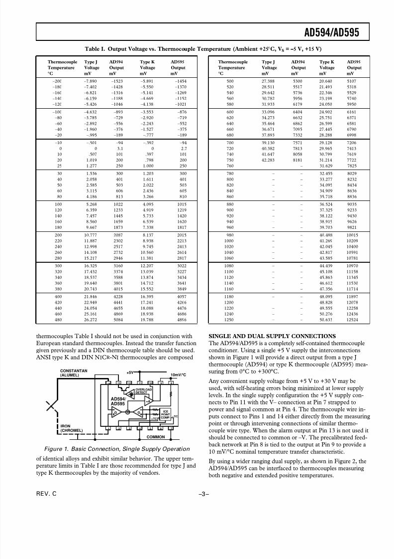
Figure 1. Basic Connection, Single Supply Operation
of identical alloys and exhibit similar behavior. The upper tem-
perature limits in Table I are those recommended for type J and
type K thermocouples by the majority of vendors.
SINGLE AND DUAL SUPPLY CONNECTIONS
The AD594/AD595 is a completely self-contained thermocouple
conditioner. Using a single +5 V supply the interconnections
shown in Figure 1 will provide a direct output from a type J
thermocouple (AD594) or type K thermocouple (AD595) mea-
suring from 0°C to +300°C.
Any convenient supply voltage from +5 V to +30 V may be
used, with self-heating errors being minimized at lower supply
levels. In the single supply configuration the +5 V supply con-
nects to Pin 11 with the V– connection at Pin 7 strapped to
power and signal common at Pin 4. The thermocouple wire in-
puts connect to Pins 1 and 14 either directly from the measuring
point or through intervening connections of similar thermo-
couple wire type. When the alarm output at Pin 13 is not used it
should be connected to common or –V. The precalibrated feed-
back network at Pin 8 is tied to the output at Pin 9 to provide a
10 mV/°C nominal temperature transfer characteristic.
By using a wider ranging dual supply, as shown in Figure 2, the
AD594/AD595 can be interfaced to thermocouples measuring
both negative and extended positive temperatures.
8/9/2019 Hoja de Catálogo Amplificador AD594
http://slidepdf.com/reader/full/hoja-de-catalogo-amplificador-ad594 4/8
AD594/AD595
REV. C–4–
CONSTANTAN(ALUMEL)
IRON(CHROMEL)
+5V TO +30V
COMMON
SPAN OF5V TO 30V
0V TO –25V
OVERLOADDETECT
G –TC
+TC
1 2 3 4 5 6 7
13 12 11 10
AD594/AD595
14
ICEPOINT
COMP.
+A
9 8
G
Figure 2. Dual Supply Operation
With a negative supply the output can indicate negative tem-
peratures and drive grounded loads or loads returned to positive
voltages. Increasing the positive supply from 5 V to 15 V ex-
tends the output voltage range well beyond the 750°C
temperature limit recommended for type J thermocouples
(AD594) and the 1250°C for type K thermocouples (AD595).
Common-mode voltages on the thermocouple inputs must remainwithin the common-mode range of the AD594/AD595, with a
return path provided for the bias currents. If the thermocouple
is not remotely grounded, then the dotted line connections in
Figures 1 and 2 are recommended. A resistor may be needed in
this connection to assure that common-mode voltages induced
in the thermocouple loop are not converted to normal mode.
THERMOCOUPLE CONNECTIONS
The isothermal terminating connections of a pair of thermo-
couple wires forms an effective reference junction. This junction
must be kept at the same temperature as the AD594/AD595 for
the internal cold junction compensation to be effective.
A method that provides for thermal equilibrium is the printedcircuit board connection layout illustrated in Figure 3.
IRON(CHROMEL)
CONSTANTAN(ALUMEL)
+T +C
–T –C
+IN –IN
1 14
–ALM+ALM
7 8COMP
COMMON V– VOUT V+
Figure 3. PCB Connections
Here the AD594/AD595 package temperature and circuit board
are thermally contacted in the copper printed circuit board
tracks under Pins 1 and 14. The reference junction is now com-
posed of a copper-constantan (or copper-alumel) connection
and copper-iron (or copper-chromel) connection, both of which
are at the same temperature as the AD594/AD595.
The printed circuit board layout shown also provides for place-
ment of optional alarm load resistors, recalibration resistors and
a compensation capacitor to limit bandwidth.
To ensure secure bonding the thermocouple wire should be
cleaned to remove oxidation prior to soldering. Noncorrosive
rosin flux is effective with iron, constantan, chromel and alumel
and the following solders: 95% tin-5% antimony, 95% tin-5%
silver or 90% tin-10% lead.
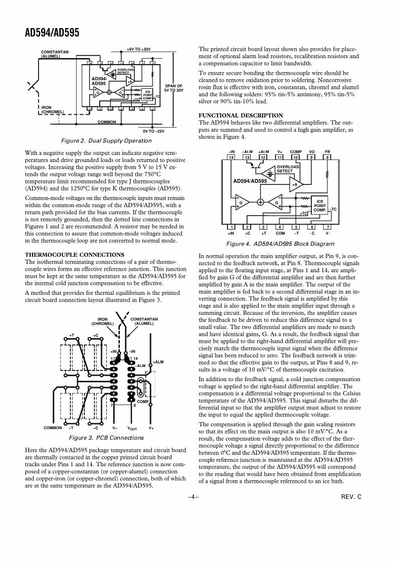
FUNCTIONAL DESCRIPTION
The AD594 behaves like two differential amplifiers. The out-
puts are summed and used to control a high gain amplifier, as
shown in Figure 4.
14 13 12 11 10 9 8
OVERLOADDETECT
ICEPOINTCOMP.
+A
GG
–TC+TC
1 2 3 4 5 6 7
AD594/AD595
+IN +C +T COM –T –C V–
–IN –ALM +ALM V+ COMP VO FB
Figure 4. AD594/AD595 Block Diagram
In normal operation the main amplifier output, at Pin 9, is con-
nected to the feedback network, at Pin 8. Thermocouple signals
applied to the floating input stage, at Pins 1 and 14, are ampli-
fied by gain G of the differential amplifier and are then further
amplified by gain A in the main amplifier. The output of the
main amplifier is fed back to a second differential stage in an in-
verting connection. The feedback signal is amplified by this
stage and is also applied to the main amplifier input through a
summing circuit. Because of the inversion, the amplifier causes
the feedback to be driven to reduce this difference signal to a
small value. The two differential amplifiers are made to match
and have identical gains, G. As a result, the feedback signal that
must be applied to the right-hand differential amplifier will pre-
cisely match the thermocouple input signal when the difference
signal has been reduced to zero. The feedback network is trim-
med so that the effective gain to the output, at Pins 8 and 9, re-
sults in a voltage of 10 mV/°C of thermocouple excitation.
In addition to the feedback signal, a cold junction compensation
voltage is applied to the right-hand differential amplifier. The
compensation is a differential voltage proportional to the Celsiustemperature of the AD594/AD595. This signal disturbs the dif-
ferential input so that the amplifier output must adjust to restore
the input to equal the applied thermocouple voltage.
The compensation is applied through the gain scaling resistors
so that its effect on the main output is also 10 mV/°C. As a
result, the compensation voltage adds to the effect of the ther-
mocouple voltage a signal directly proportional to the difference
between 0°C and the AD594/AD595 temperature. If the thermo-
couple reference junction is maintained at the AD594/AD595
temperature, the output of the AD594/AD595 will correspond
to the reading that would have been obtained from amplification
of a signal from a thermocouple referenced to an ice bath.

8/9/2019 Hoja de Catálogo Amplificador AD594
http://slidepdf.com/reader/full/hoja-de-catalogo-amplificador-ad594 5/8
AD594/AD595
REV. C –5–
The AD594/AD595 also includes an input open circuit detector
that switches on an alarm transistor. This transistor is actually a
current-limited output buffer, but can be used up to the limit as
a switch transistor for either pull-up or pull-down operation of
external alarms.
The ice point compensation network has voltages available with
positive and negative temperature coefficients. These voltages
may be used with external resistors to modify the ice point com-
pensation and recalibrate the AD594/AD595 as described in the
next column.
The feedback resistor is separately pinned out so that its value
can be padded with a series resistor, or replaced with an external
resistor between Pins 5 and 9. External availability of the feedback
resistor allows gain to be adjusted, and also permits the AD594/
AD595 to operate in a switching mode for setpoint operation.
CAUTIONS:
The temperature compensation terminals (+C and –C) at Pins 2
and 6 are provided to supply small calibration currents only. The
AD594/AD595 may be permanently damaged if they are
grounded or connected to a low impedance.The AD594/AD595 is internally frequency compensated for feed-
back ratios (corresponding to normal signal gain) of 75 or more.
If a lower gain is desired, additional frequency compensation
should be added in the form of a 300 pF capacitor from Pin 10
to the output at Pin 9. As shown in Figure 5 an additional 0.01 µF
capacitor between Pins 10 and 11 is recommended.
AD594/AD595
VO
COMP
+V
9
10
11
300pF
0.01F
Figure 5. Low Gain Frequency Compensation
RECALIBRATION PRINCIPLES AND LIMITATIONS
The ice point compensation network of the AD594/AD595
produces a differential signal which is zero at 0°C and corre-
sponds to the output of an ice referenced thermocouple at the
temperature of the chip. The positive TC output of the circuit is
proportional to Kelvin temperature and appears as a voltage at
+T. It is possible to decrease this signal by loading it with a
resistor from +T to COM, or increase it with a pull-up resistor
from +T to the larger positive TC voltage at +C. Note that
adjustments to +T should be made by measuring the voltage which
tracks it at –T. To avoid destabilizing the feedback amplifier the
measuring instrument should be isolated by a few thousand
ohms in series with the lead connected to –T.
AD594/AD595
+IN
–IN
+T
COM
–T
FB
VO9
1
14
8
3
4
5
Figure 6. Decreased Sensitivity Adjustment
Changing the positive TC half of the differential output of the
compensation scheme shifts the zero point away from 0°C. The
zero can be restored by adjusting the current flow into the nega-
tive input of the feedback amplifier, the –T pin. A current into
this terminal can be produced with a resistor between –C and
–T to balance an increase in +T, or a resistor from –T to COM
to offset a decrease in +T.
If the compensation is adjusted substantially to accommodate a
different thermocouple type, its effect on the final output volt-
age will increase or decrease in proportion. To restore the
nominal output to 10 mV/°C the gain may be adjusted to match
the new compensation and thermocouple input characteristics.
When reducing the compensation the resistance between –T
and COM automatically increases the gain to within 0.5% of the
correct value. If a smaller gain is required, however, the nomina
47 kΩ internal feedback resistor can be paralleled or replaced
with an external resistor.
Fine calibration adjustments will require temperature response
measurements of individual devices to assure accuracy. Major
reconfigurations for other thermocouple types can be achieved
without seriously compromising initial calibration accuracy, so
long as the procedure is done at a fixed temperature using the
factory calibration as a reference. It should be noted that inter-
mediate recalibration conditions may require the use of a
negative supply.
EXAMPLE: TYPE E RECALIBRATION—AD594/AD595
Both the AD594 and AD595 can be configured to condition the
output of a type E (chromel-constantan) thermocouple. Tem-
perature characteristics of type E thermocouples differ less from
type J, than from type K, therefore the AD594 is preferred for
recalibration.
While maintaining the device at a constant temperature follow
the recalibration steps given here. First, measure the device
temperature by tying both inputs to common (or a selected
common-mode potential) and connecting FB to VO. The AD594
is now in the stand alone Celsius thermometer mode. For this
example assume the ambient is 24°C and the initial output VO
is 240 mV. Check the output at VO to verify that it correspondsto the temperature of the device.
Next, measure the voltage –T at Pin 5 with a high impedance
DVM (capacitance should be isolated by a few thousand ohms
of resistance at the measured terminals). At 24°C the –T voltage
will be about 8.3 mV. To adjust the compensation of an AD594
to a type E thermocouple a resistor, R1, should be connected
between +T and +C, Pins 2 and 3, to raise the voltage at –T by
the ratio of thermocouple sensitivities. The ratio for converting a
type J device to a type E characteristic is:
r ( AD594) =(60.9 µV /°C )/(51.7 µV /°C )= 1.18
Thus, multiply the initial voltage measured at –T by r and ex-
perimentally determine the R1 value required to raise –T to that
level. For the example the new –T voltage should be about 9.8 mVThe resistance value should be approximately 1.8 kΩ.
The zero differential point must now be shifted back to 0°C.
This is accomplished by multiplying the original output voltage
VO by r and adjusting the measured output voltage to this value
by experimentally adding a resistor, R2, between –C and –T,
Pins 5 and 6. The target output value in this case should be
about 283 mV. The resistance value of R2 should be approxi-
mately 240 kΩ.
Finally, the gain must be recalibrated such that the output VO
indicates the device’s temperature once again. Do this by adding
a third resistor, R3, between FB and –T, Pins 8 and 5. VO should
now be back to the initial 240 mV reading. The resistance value

8/9/2019 Hoja de Catálogo Amplificador AD594
http://slidepdf.com/reader/full/hoja-de-catalogo-amplificador-ad594 6/8
AD594/AD595
REV. C–6–
of R3 should be approximately 280 kΩ. The final connection
diagram is shown in Figure 7. An approximate verification of
the effectiveness of recalibration is to measure the differential
gain to the output. For type E it should be 164.2.
AD594/AD595
–T
+IN
–IN +T
COM1
14
4
2
3
–C
5
6
FB
VO
8
9
R3
+C
R1
R2
Figure 7. Type E Recalibration
When implementing a similar recalibration procedure for the
AD595 the values for R1, R2, R3 and r will be approximately
650 Ω, 84 kΩ, 93 kΩ and 1.51, respectively. Power consump-
tion will increase by about 50% when using the AD595 withtype E inputs.
Note that during this procedure it is crucial to maintain the
AD594/AD595 at a stable temperature because it is used as the
temperature reference. Contact with fingers or any tools not at
ambient temperature will quickly produce errors. Radiational
heating from a change in lighting or approach of a soldering iron
must also be guarded against.
USING TYPE T THERMOCOUPLES WITH THE AD595
Because of the similarity of thermal EMFs in the 0°C to +50°C
range between type K and type T thermocouples, the AD595
can be directly used with both types of inputs. Within this ambi-
ent temperature range the AD595 should exhibit no more than
an additional 0.2°C output calibration error when used withtype T inputs. The error arises because the ice point compensa-
tor is trimmed to type K characteristics at 25°C. To calculate
the AD595 output values over the recommended –200°C to
+350°C range for type T thermocouples, simply use the ANSI
thermocouple voltages referred to 0°C and the output equation
given on page 2 for the AD595. Because of the relatively large
nonlinearities associated with type T thermocouples the output
will deviate widely from the nominal 10 mV/°C. However, cold
junction compensation over the rated 0°C to +50°C ambient
will remain accurate.
STABILITY OVER TEMPERATURE
Each AD594/AD595 is tested for error over temperature with
the measuring thermocouple at 0°C. The combined effects of
cold junction compensation error, amplifier offset drift and gain
error determine the stability of the AD594/AD595 output over
the rated ambient temperature range. Figure 8 shows an AD594/
AD595 drift error envelope. The slope of this figure has units
of °C/°C.
TEMPERATURE OF AD594C/AD595C –0.6C D R I F T E R R O R
50C25C
0
+0.6C
Figure 8. Drift Error vs. Temperature
THERMAL ENVIRONMENT EFFECTS
The inherent low power dissipation of the AD594/AD595 and
the low thermal resistance of the package make self-heating
errors almost negligible. For example, in still air the chip to am-
bient thermal resistance is about 80°C/watt (for the D package).
At the nominal dissipation of 800 µW the self-heating in free air
is less than 0.065°C. Submerged in fluorinert liquid (unstirred)
the thermal resistance is about 40°C/watt, resulting in a self-heating error of about 0.032°C.
SETPOINT CONTROLLER
The AD594/AD595 can readily be connected as a setpoint
controller as shown in Figure 9.
CONSTANTAN(ALUMEL)
IRON(CHROMEL)
+5V
COMMON
HEATER
20M(OPTIONAL)FORHYSTERESIS
SETPOINTVOLTAGEINPUT
TEMPERATURECONTROLLEDREGION
LOW = > T < SETPOINTHIGH = > T > SETPOINTTEMPERATURE
COMPARATOR OUT
HEATERDRIVER
OVERLOADDETECT
G –TC
+TC
1 2 3 4 5 6 7
13 12 11 10
AD594/AD595
14
ICEPOINTCOMP.
+A
9 8
G
Figure 9. Setpoint Controller
The thermocouple is used to sense the unknown temperature
and provide a thermal EMF to the input of the AD594/AD595.
The signal is cold junction compensated, amplified to 10 mV/°C
and compared to an external setpoint voltage applied by the
user to the feedback at Pin 8. Table I lists the correspondence
between setpoint voltage and temperature, accounting for the
nonlinearity of the measurement thermocouple. If the setpoint
temperature range is within the operating range (–55°C to
+125°C) of the AD594/AD595, the chip can be used as the
transducer for the circuit by shorting the inputs together and
utilizing the nominal calibration of 10 mV/°C. This is the centi-
grade thermometer configuration as shown in Figure 13.
In operation if the setpoint voltage is above the voltage corre-
sponding to the temperature being measured the output swings
low to approximately zero volts. Conversely, when the tempera-
ture rises above the setpoint voltage the output switches to
the positive limit of about 4 volts with a +5 V supply. Figure
9 shows the setpoint comparator configuration complete with a
heater element driver circuit being controlled by the AD594/
AD595 toggled output. Hysteresis can be introduced by inject-ing a current into the positive input of the feedback amplifier
when the output is toggled high. With an AD594 about 200 nA
into the +T terminal provides 1°C of hysteresis. When using a
single 5 V supply with an AD594, a 20 MΩ resistor from VO to
+T will supply the 200 nA of current when the output is forced
high (about 4 V). To widen the hysteresis band decrease the
resistance connected from VO to +T.

8/9/2019 Hoja de Catálogo Amplificador AD594
http://slidepdf.com/reader/full/hoja-de-catalogo-amplificador-ad594 7/8
AD594/AD595
REV. C –7–
ALARM CIRCUIT
In all applications of the AD594/AD595 the –ALM connection,
Pin 13, should be constrained so that it is not more positive
than (V+) – 4 V. This can be most easily achieved by connect-
ing Pin 13 to either common at Pin 4 or V– at Pin 7. For most
applications that use the alarm signal, Pin 13 will be grounded
and the signal will be taken from +ALM on Pin 12. A typical
application is shown in Figure 10.
In this configuration the alarm transistor will be off in normal
operation and the 20 k pull up will cause the +ALM output on
Pin 12 to go high. If one or both of the thermocouple leads are
interrupted, the +ALM pin will be driven low. As shown in Fig-
ure 10 this signal is compatible with the input of a TTL gate
which can be used as a buffer and/or inverter.
CONSTANTAN(ALUMEL)
IRON(CHROMEL)
+5V
ALARMTTL GATE
20k ALARM OUT
GND
OVERLOADDETECT
G –TC
+TC
1 2 3 4 5 6 7
13 12 11 10
AD594/AD595
14
ICEPOINTCOMP.
+A
9 8
G
10mV/C
Figure 10. Using the Alarm to Drive a TTL Gate
(“Grounded’’ Emitter Configuration)
Since the alarm is a high level output it may be used to directly
drive an LED or other indicator as shown in Figure 11.
CONSTANTAN(ALUMEL)
IRON(CHROMEL)
COMMON
LED
270
V+
OVERLOADDETECT
G –TC
+TC
1 2 3 4 5 6 7
13 12 11 10
AD594/AD595
14
ICEPOINTCOMP.
+A
9 8
G
10mV/C
Figure 11. Alarm Directly Drives LED
A 270 Ω series resistor will limit current in the LED to 10 mA,but may be omitted since the alarm output transistor is current
limited at about 20 mA. The transistor, however, will operate in
a high dissipation mode and the temperature of the circuit will
rise well above ambient. Note that the cold junction compensa-
tion will be affected whenever the alarm circuit is activated. The
time required for the chip to return to ambient temperature will
depend on the power dissipation of the alarm circuit, the nature
of the thermal path to the environment and the alarm duration.
The alarm can be used with both single and dual supplies. It
can be operated above or below ground. The collector and emit-
ter of the output transistor can be used in any normal switch
configuration. As an example a negative referenced load can be
driven from –ALM as shown in Figure 12.
CONSTANTAN
(ALUMEL)
IRON(CHROMEL)
+10V
GND
ALARMRELAY –12V
OVERLOADDETECT
G –TC
+TC
1 2 3 4 5 6 7
13 12 11 10
AD594/AD595
14
ICEPOINTCOMP.
+A
9 8
G
10mV/C
Figure 12. –ALM Driving A Negative Referenced Load
The collector (+ALM) should not be allowed to become more
positive than (V–) +36 V, however, it may be permitted to be
more positive than V+. The emitter voltage (–ALM) should be
constrained so that it does not become more positive than 4
volts below the V+ applied to the circuit.
Additionally, the AD594/AD595 can be configured to produce
an extreme upscale or downscale output in applications where
an extra signal line for an alarm is inappropriate. By tying either
of the thermocouple inputs to common most runaway control
conditions can be automatically avoided. A +IN to common
connection creates a downscale output if the thermocouple opens,
while connecting –IN to common provides an upscale output.
CELSIUS THERMOMETER
The AD594/AD595 may be configured as a stand-alone Celsius
thermometer as shown in Figure 13.
+5V TO +15V
OUTPUT10mV/C
GND0 TO –15V
OVERLOADDETECT
G –TC
+TC
1 2 3 4 5 6 7
13 12 11 10
AD594/AD595
14
ICEPOINTCOMP.
+A
9 8
G
Figure 13. AD594/AD595 as a Stand-Alone Celsius
Thermometer
Simply omit the thermocouple and connect the inputs (Pins 1
and 14) to common. The output now will reflect the compensa-
tion voltage and hence will indicate the AD594/AD595
temperature with a scale factor of 10 mV/°C. In this three termi-
nal, voltage output, temperature sensing mode, the AD594/
AD595 will operate over the full military –55°C to +125°C tem-
perature range.

8/9/2019 Hoja de Catálogo Amplificador AD594
http://slidepdf.com/reader/full/hoja-de-catalogo-amplificador-ad594 8/8
AD594/AD595
REV. C–8–
OUTLINE DIMENSIONS
Dimensions shown in inches and (mm).
TO-116 (D) Package
0.100(2.54)BSC
0.700 ±0.010(17.78 ±0.25)
0.180 ±0.030(4.57 ±0.76)
0.085 (2.16)
0.035 ±0.010(0.89 ±0.25)
0.047 ±0.007(1.19 ±0.18)
0.017 +0.003 –0.002
0.43 +0.08 –0.05( (
0.125(3.18)
MIN
0.31 ±0.01(7.87 ±0.25)
0.01 ±0.002(0.25 ±0.05)
0.095 (2.41)
0.30 (7.62) REF
0.430 (10.92)
14
1 7
80.040
(1.02) R
PIN 1
0.265(6.73)
0.290 ±0.010(7.37 ±0.25)
Cerdip (Q) Package
14
1 7
8
PIN 1
0.77 ±0.015
(19.55 ±0.39)
0.310(7.87)
0.260 ±0.020(6.6 ±0.51)
SEATINGPLANE
0.100(2.54)BSC
0.035 ±0.010(0.889 ±0.254)
0.180 ±0.030(4.57 ±0.76)
0.1253.175)
MIN
0.032(0.812)
15°0°
0.300 (7.62)REF
0.148 ±0.015(3.76 ±0.38)
0.010 ±0.001(0.254 ±0.025)0.018
(0.457)
0.600 (15.24)BSC
THERMOCOUPLE BASICS
Thermocouples are economical and rugged; they have reason-
ably good long-term stability. Because of their small size, they
respond quickly and are good choices where fast response is im-
portant. They function over temperature ranges from cryogenics
to jet-engine exhaust and have reasonable linearity and accuracy.
Because the number of free electrons in a piece of metal de-
pends on both temperature and composition of the metal, two
pieces of dissimilar metal in isothermal and contact will exhibit
a potential difference that is a repeatable function of tempera-
ture, as shown in Figure 14. The resulting voltage depends on
the temperatures, T1 and T2, in a repeatable way.
CONSTANTAN
IRON
UNKNOWNTEMPERATURE
ICE POINTREFERENCE
T1 T2
CONSTANTANCu Cu
V1
Figure 14. Thermocouple Voltage with 0 °C Reference
Since the thermocouple is basically a differential rather than
absolute measuring device, a know reference temperature is
required for one of the junctions if the temperature of the other
is to be inferred from the output voltage. Thermocouples made
of specially selected materials have been exhaustively character-
ized in terms of voltage versus temperature compared to primary
temperature standards. Most notably the water-ice point of 0°C
is used for tables of standard thermocouple performance.
An alternative measurement technique, illustrated in Figure 15,
is used in most practical applications where accuracy requirements
do not warrant maintenance of primary standards. The referencejunction temperature is allowed to change with the environment
of the measurement system, but it is carefully measured by some
type of absolute thermometer. A measurement of the thermo-
couple voltage combined with a knowledge of the reference
temperature can be used to calculate the measurement junction
temperature. Usual practice, however, is to use a convenient
thermoelectric method to measure the reference temperature
and to arrange its output voltage so that it corresponds to a ther-
mocouple referred to 0°C. This voltage is simply added to the
thermocouple voltage and the sum then corresponds to the stan-
dard voltage tabulated for an ice-point referenced thermocouple.
CONSTANTAN
IRON
T1
V1
CuNi–Cu Cu
T3
V1' = V1
FOR PROPERLY
SCALED V3' = f(T
3)
V3'
V1'
V2
Figure 15. Substitution of Measured Reference
Temperature for Ice Point Reference
The temperature sensitivity of silicon integrated circuit transis-
tors is quite predictable and repeatable. This sensitivity is
exploited in the AD594/AD595 to produce a temperature re-lated voltage to compensate the reference of “cold” junction of a
thermocouple as shown in Figure 16.
Cu
CONSTANTAN
IRON
T1
Cu
T3
Figure 16. Connecting Isothermal Junctions
Since the compensation is at the reference junction temperature,
it is often convenient to form the reference “junction” by connect-
ing directly to the circuit wiring. So long as these connections
and the compensation are at the same temperature no error will
result.